Register once, drag and drop ECAD models into your CAD tool and speed up your design.
Click here for more information74AUP2G132GM
Low-power dual 2-input NAND Schmitt trigger
The 74AUP2G132 is a dual 2-input NAND gate with Schmitt-trigger inputs. This device ensures very low static and dynamic power consumption across the entire VCC range from 0.8 V to 3.6 V. This device is fully specified for partial power down applications using IOFF. The IOFF circuitry disables the output, preventing the potentially damaging backflow current through the device when it is powered down.
Alternatives
Features and benefits
Wide supply voltage range from 0.8 V to 3.6 V
CMOS low power dissipation
High noise immunity
Low static power consumption; ICC = 0.9 μA (maximum)
Latch-up performance exceeds 100 mA per JESD 78 Class II Level B
Overvoltage tolerant inputs to 3.6 V
Low noise overshoot and undershoot < 10 % of VCC
IOFF circuitry provides partial Power-down mode operation
Complies with JEDEC standards:
JESD8-12 (0.8 V to 1.3 V)
JESD8-11 (0.9 V to 1.65 V)
JESD8-7 (1.65 V to 1.95 V)
JESD8-5 (2.3 V to 2.7 V)
JESD8C (2.7 V to 3.6 V)
ESD protection:
HBM: ANSI/ESDA/JEDEC JS-001 class 3A exceeds 5000 V
CDM: ANSI/ESDA/JEDEC JS-002 class C3 exceeds 1000 V
Multiple package options
Specified from -40 °C to +85 °C and -40 °C to +125 °C
Applications
Wave and pulse shaper
Astable multivibrator
Monostable multivibrator
参数类型
| 型号 | Product status | Package name |
|---|---|---|
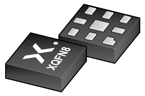
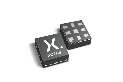
| 74AUP2G132GM | End of life | XQFN8 |
PCB Symbol, Footprint and 3D Model
| Model Name | 描述 |
|---|---|
|
|
封装
下表中的所有产品型号均已停产 。
| 型号 | 可订购的器件编号,(订购码(12NC)) | 状态 | 标示 | 封装 | 外形图 | 回流焊/波峰焊 | 包装 |
|---|---|---|---|---|---|---|---|
| 74AUP2G132GM | 74AUP2G132GM,125 (935281435125) |
Obsolete | aE2 |
XQFN8 (SOT902-2) |
SOT902-2 | SOT902-2_125 |
环境信息
下表中的所有产品型号均已停产 。
| 型号 | 可订购的器件编号 | 化学成分 | RoHS | RHF指示符 |
|---|---|---|---|---|
| 74AUP2G132GM | 74AUP2G132GM,125 | 74AUP2G132GM |
|
|
Series
文档 (9)
| 文件名称 | 标题 | 类型 | 日期 |
|---|---|---|---|
| 74AUP2G132 | Low-power dual 2-input NAND Schmitt trigger | Data sheet | 2023-07-26 |
| AN10161 | PicoGate Logic footprints | Application note | 2002-10-29 |
| AN11052 | Pin FMEA for AUP family | Application note | 2019-01-09 |
| Nexperia_document_guide_MiniLogic_MicroPak_201808 | MicroPak leadless logic portfolio guide | Brochure | 2018-09-03 |
| aup2g132 | aup2g132 IBIS model | IBIS model | 2013-04-08 |
| Nexperia_document_leaflet_Logic_AUP_technology_portfolio_201904 | Nexperia_document_leaflet_Logic_AUP_technology_portfolio_201904 | Leaflet | 2019-04-12 |
| Nexperia_package_poster | Nexperia package poster | Leaflet | 2020-05-15 |
| XQFN8_SOT902-2_mk | plastic, extremely thin quad flat package; 8 terminals; 0.55 mm pitch; 1.6 mm x 1.6 mm x 0.5 mm body | Marcom graphics | 2017-01-28 |
| SOT902-2 | plastic, leadless extremely thin quad flat package; 8 terminals; 0.5 mm pitch; 1.6 mm x 1.6 mm x 0.5 mm body | Package information | 2020-04-21 |
支持
如果您需要设计/技术支持,请告知我们并填写 应答表 我们会尽快回复您。
模型
| 文件名称 | 标题 | 类型 | 日期 |
|---|---|---|---|
| aup2g132 | aup2g132 IBIS model | IBIS model | 2013-04-08 |
PCB Symbol, Footprint and 3D Model
| Model Name | 描述 |
|---|---|
|
|
How does it work?
The interactive datasheets are based on the Nexperia MOSFET precision electrothermal models. With our interactive datasheets you can simply specify your own conditions interactively. Start by changing the values of the conditions. You can do this by using the sliders in the condition fields. By dragging the sliders you will see how the MOSFET will perform at the new conditions set.
74AUP2G132GM
Low-power dual 2-input NAND Schmitt trigger
从安世半导体购买
| SKU | 库存* | MOQ | 单位价格 | 数量 |
|---|