Register once, drag and drop ECAD models into your CAD tool and speed up your design.
Click here for more information74LVC30APW
8-input NAND gate
The 74LVC30A is an 8-input NAND gate.
Inputs can be driven from either 3.3 V or 5 V devices. This feature allows the use of these devices in a mixed 3.3 V and 5 V environment.
Schmitt trigger action at all inputs makes the circuit tolerant for slower input rise and fall time.
This device is fully specified for partial power-down applications using IOFF. The IOFF circuitry disables the output, preventing the damaging backflow current through the device when it is powered down.
Features and benefits
Wide supply voltage range from 1.2 V to 3.6 V
Inputs accept voltages up to 5.5 V
CMOS low power consumption
Direct interface with TTL levels
Complies with JEDEC standard:
JESD8-7A (1.65 V to 1.95 V)
JESD8-5A (2.3 V to 2.7 V)
JESD8-C/JESD36 (2.7 V to 3.6 V)
ESD protection:
HBM JEDEC JS-001-2012 exceeds 2000 V
MM JESD22-A115-C exceeds 200 V
CDM JESD22-C101F exceeds 1000 V
Specified from ‑40 °C to +85 °C and ‑40 °C to +125 °C
Applications
参数类型
| 型号 | Product status | VCC (V) | Logic switching levels | Output drive capability (mA) | tpd (ns) | fmax (MHz) | Nr of bits | Power dissipation considerations | Tamb (°C) | Rth(j-a) (K/W) | Ψth(j-top) (K/W) | Rth(j-c) (K/W) | Package name |
|---|---|---|---|---|---|---|---|---|---|---|---|---|---|
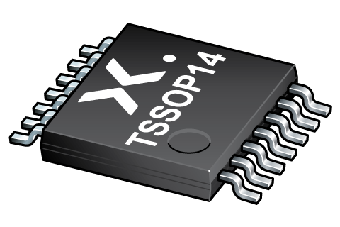
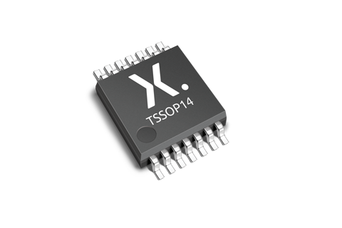
| 74LVC30APW | End of life | 1.65 - 5.5 | CMOS/LVTTL | ± 24 | 3.6 | 175 | 1 | low | -40~125 | 144 | 8.8 | 71 | TSSOP14 |
封装
下表中的所有产品型号已停产。参见表 停产信息 了解更多信息。
| 型号 | 可订购的器件编号,(订购码(12NC)) | 状态 | 标示 | 封装 | 外形图 | 回流焊/波峰焊 | 包装 |
|---|---|---|---|---|---|---|---|
| 74LVC30APW | 74LVC30APWJ (935304017118) |
Obsolete | LVC30A |
TSSOP14 (SOT402-1) |
SOT402-1 |
SSOP-TSSOP-VSO-WAVE
|
SOT402-1_118 |
环境信息
下表中的所有产品型号已停产。参见表 停产信息 了解更多信息。
| 型号 | 可订购的器件编号 | 化学成分 | RoHS | RHF指示符 |
|---|---|---|---|---|
| 74LVC30APW | 74LVC30APWJ | 74LVC30APW |
|
|
文档 (8)
| 文件名称 | 标题 | 类型 | 日期 |
|---|---|---|---|
| 74LVC30A | 8-input NAND gate | Data sheet | 2019-03-15 |
| SOT402-1 | 3D model for products with SOT402-1 package | Design support | 2023-02-02 |
| SOT402 | 3D model for products with SOT402 package | Design support | 2020-01-22 |
| lvc30a | lvc30a IBIS model | IBIS model | 2018-11-29 |
| Nexperia_package_poster | Nexperia package poster | Leaflet | 2020-05-15 |
| TSSOP14_SOT402-1_mk | plastic, thin shrink small outline package; 14 leads; 0.65 mm pitch; 5 mm x 4.4 mm x 1.1 mm body | Marcom graphics | 2017-01-28 |
| SOT402-1 | plastic, thin shrink small outline package; 14 leads; 0.65 mm pitch; 5 mm x 4.4 mm x 1.2 mm body | Package information | 2023-11-07 |
| SSOP-TSSOP-VSO-WAVE | Footprint for wave soldering | Wave soldering | 2009-10-08 |
支持
如果您需要设计/技术支持,请告知我们并填写 应答表 我们会尽快回复您。
How does it work?
The interactive datasheets are based on the Nexperia MOSFET precision electrothermal models. With our interactive datasheets you can simply specify your own conditions interactively. Start by changing the values of the conditions. You can do this by using the sliders in the condition fields. By dragging the sliders you will see how the MOSFET will perform at the new conditions set.
74LVC30APW
8-input NAND gate
从安世半导体购买
| SKU | 库存* | MOQ | 单位价格 | 数量 |
|---|