可订购部件
| 型号 | 可订购的器件编号 | 订购代码(12NC) | 封装 | 从经销商处购买 |
|---|---|---|---|---|
| 74LV165APW | 74LV165APW,118 | 935273177118 | SOT403-1 | 订单产品 |

Register once, drag and drop ECAD models into your CAD tool and speed up your design.
Click here for more information8-bit parallel-in/serial-out shift register
74LV165A是8位并行负载或串行输入移位寄存器,末级提供互补串行输出(Q7和Q7)。并行负载(PL)输入为低电平时,来自D0至D7输入的并行数据会异步加载到寄存器中。输入PL为高电平时,数据在输入DS处串行输入寄存器。其随每次时钟正向跃迁向右移一位(Q0 → Q1 → Q2,以此类推)。通过将Q7输出连接到后一级的DS输入,该特性可实现并行到串行转换器扩展。
时钟输入为门控或结构,允许一个输入用作低电平有效时钟使能输入(CE)输入。CP和CE输入的针脚分配是任意的,为方便布局可颠倒。CE输入从低电平至高电平的跃迁应当仅在CP为高电平时发生,以便操作可预测。
所有输入的施密特触发器动作使电路容许较慢的输入上升和下降时间。其完全适合使用IOFF的局部掉电应用。IOFF电路可禁用输出,防止掉电时破坏性回流电流通过该器件。
| 型号 | Product status | VCC (V) | Logic switching levels | Output drive capability (mA) | tpd (ns) | fmax (MHz) | Nr of bits | Power dissipation considerations | Tamb (°C) | Rth(j-a) (K/W) | Ψth(j-top) (K/W) | Rth(j-c) (K/W) | Package name |
|---|---|---|---|---|---|---|---|---|---|---|---|---|---|
| 74LV165APW | Production | 1.0 - 5.5 | TTL | ± 12 | 7.5 | 115 | 8 | low | -40~85 | 124 | 4.4 | 53.9 | TSSOP16 |
| Model Name | 描述 |
|---|---|
|
|
| 型号 | 可订购的器件编号,(订购码(12NC)) | 状态 | 标示 | 封装 | 外形图 | 回流焊/波峰焊 | 包装 |
|---|---|---|---|---|---|---|---|
| 74LV165APW | 74LV165APW,118 (935273177118) |
Active | LV165A |
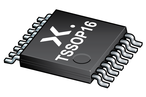
TSSOP16 (SOT403-1) |
SOT403-1 |
SSOP-TSSOP-VSO-WAVE
|
SOT403-1_118 |
| 文件名称 | 标题 | 类型 | 日期 |
|---|---|---|---|
| 74LV165A | 8-bit parallel-in/serial-out shift register | Data sheet | 2017-04-07 |
| SOT403-1 | 3D model for products with SOT403-1 package | Design support | 2020-01-22 |
| Nexperia_package_poster | Nexperia package poster | Leaflet | 2020-05-15 |
| TSSOP16_SOT403-1_mk | plastic, thin shrink small outline package; 16 leads; 0.65 mm pitch; 5 mm x 4.4 mm x 1.1 mm body | Marcom graphics | 2017-01-28 |
| SOT403-1 | plastic, thin shrink small outline package; 16 leads; 5 mm x 4.4 mm x 1.2 mm body | Package information | 2023-11-08 |
| SOT403-1_118 | TSSOP16; Reel pack for SMD, 13"; Q1/T1 product orientation | Packing information | 2020-04-21 |
| 74LV165APW_Nexperia_Product_Reliability | 74LV165APW Nexperia Product Reliability | Quality document | 2023-05-29 |
| SSOP-TSSOP-VSO-WAVE | Footprint for wave soldering | Wave soldering | 2009-10-08 |
如果您需要设计/技术支持,请告知我们并填写 应答表 我们会尽快回复您。
| 文件名称 | 标题 | 类型 | 日期 |
|---|---|---|---|
| SOT403-1 | 3D model for products with SOT403-1 package | Design support | 2020-01-22 |
| Model Name | 描述 |
|---|---|
|
|
| 型号 | Orderable part number | Ordering code (12NC) | 状态 | 包装 | Packing Quantity | 在线购买 |
|---|---|---|---|---|---|---|
| 74LV165APW | 74LV165APW,118 | 935273177118 | Active | SOT403-1_118 | 2,500 | 订单产品 |
安世半导体客户可通过我们的销售机构或直接通过在线样品商店订购样品: https://extranet.nexperia.com.
样品订单通常需要2-4天寄送时间。
如果您尚未取得安世半导体的直接采购帐号,我们的全球与区域经销网络可以协助您取得样品。
The interactive datasheets are based on the Nexperia MOSFET precision electrothermal models. With our interactive datasheets you can simply specify your own conditions interactively. Start by changing the values of the conditions. You can do this by using the sliders in the condition fields. By dragging the sliders you will see how the MOSFET will perform at the new conditions set.
8-bit parallel-in/serial-out shift register
| SKU | 库存* | MOQ | 单位价格 | 数量 |
|---|