
可订购部件
| 型号 | 可订购的器件编号 | 订购代码(12NC) | 封装 | 从经销商处购买 |
|---|---|---|---|---|
| 74HCT193D | 74HCT193D,653 | 933715100653 | SOT109-1 | 订单产品 |
Register once, drag and drop ECAD models into your CAD tool and speed up your design.
Click here for more informationPresettable synchronous 4-bit binary up/down counter
The 74HC193; 74HCT193 is a 4-bit synchronous binary up/down counter. Separate up/down clocks, CPU and CPD respectively, simplify operation. The outputs change state synchronously with the LOW-to-HIGH transition of either clock input. If the CPU clock is pulsed while CPD is held HIGH, the device will count up. If the CPD clock is pulsed while CPU is held HIGH, the device will count down. Only one clock input can be held HIGH at any time to guarantee predictable behavior. The device can be cleared at any time by the asynchronous master reset input (MR); it may also be loaded in parallel by activating the asynchronous parallel load input (PL). The terminal count up (TCU) and terminal count down (TCD) outputs are normally HIGH. When the circuit has reached the maximum count state of 15, the next HIGH-to-LOW transition of CPU will cause TCU to go LOW. TCU will stay LOW until CPU goes HIGH again, duplicating the count up clock. Likewise, the TCD output will go LOW when the circuit is in the zero state and the CPD goes LOW. The terminal count outputs can be used as the clock input signals to the next higher order circuit in a multistage counter, since they duplicate the clock waveforms. Multistage counters will not be fully synchronous, since there is a slight delay time difference added for each stage that is added. The counter may be preset by the asynchronous parallel load capability of the circuit. Information present on the parallel data inputs (D0 to D3) is loaded into the counter and appears on the outputs (Q0 to Q3) regardless of the conditions of the clock inputs when the parallel load (PL) input is LOW. A HIGH level on the master reset (MR) input will disable the parallel load gates, override both clock inputs and set all outputs (Q0 to Q3) LOW. If one of the clock inputs is LOW during and after a reset or load operation, the next LOW-to-HIGH transition of that clock will be interpreted as a legitimate signal and will be counted. Inputs include clamp diodes. This enables the use of current limiting resistors to interface inputs to voltages in excess of VCC.
Wide supply voltage range from 2.0 to 6.0 V
CMOS low power dissipation
High noise immunity
Latch-up performance exceeds 100 mA per JESD 78 Class II Level B
Input levels:
For 74HC193: CMOS level
For 74HCT193: TTL level
Synchronous reversible 4-bit binary counting
Asynchronous parallel load
Asynchronous reset
Expandable without external logic
Complies with JEDEC standards:
JESD8C (2.7 V to 3.6 V)
JESD7A (2.0 V to 6.0 V)
ESD protection:
HBM: ANSI/ESDA/JEDEC JS-001 class 2 exceeds 2000 V
CDM: ANSI/ESDA/JEDEC JS-002 class C3 exceeds 1000 V
Specified from -40 °C to +85 °C and -40 °C to +125 °C.
| 型号 | Product status | VCC (V) | Output drive capability (mA) | Logic switching levels | tpd (ns) | Power dissipation considerations | Tamb (°C) | Rth(j-a) (K/W) | Ψth(j-top) (K/W) | Rth(j-c) (K/W) | Package name |
|---|---|---|---|---|---|---|---|---|---|---|---|
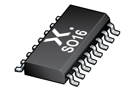
| 74HCT193D | Production | 4.5 - 5.5 | ± 4 | TTL | 20 | low | -40~125 | 66 | 1.0 | 23 | SO16 |
| Model Name | 描述 |
|---|---|
|
|
| 型号 | 可订购的器件编号,(订购码(12NC)) | 状态 | 标示 | 封装 | 外形图 | 回流焊/波峰焊 | 包装 |
|---|---|---|---|---|---|---|---|
| 74HCT193D | 74HCT193D,653 (933715100653) |
Active | 74HCT193D |
SO16 (SOT109-1) |
SOT109-1 |
SO-SOJ-REFLOW
SO-SOJ-WAVE WAVE_BG-BD-1 |
Not available |
| 文件名称 | 标题 | 类型 | 日期 |
|---|---|---|---|
| 74HC_HCT193 | Presettable synchronous 4-bit binary up/down counter | Data sheet | 2024-03-14 |
| AN11044 | Pin FMEA 74HC/74HCT family | Application note | 2019-01-09 |
| SOT109-1 | 3D model for products with SOT109-1 package | Design support | 2020-01-22 |
| hct193 | 74HCT193 IBIS model | IBIS model | 2022-10-11 |
| Nexperia_package_poster | Nexperia package poster | Leaflet | 2020-05-15 |
| SO16_SOT109-1_mk | plastic, small outline package; 16 leads; 1.27 mm pitch; 9.9 mm x 3.9 mm x 1.35 mm body | Marcom graphics | 2017-01-28 |
| SOT109-1 | plastic, small outline package; 16 leads; 1.27 mm pitch; 9.9 mm x 3.9 mm x 1.75 mm body | Package information | 2023-11-07 |
| 74HCT193D_Nexperia_Product_Reliability | 74HCT193D Nexperia Product Reliability | Quality document | 2023-05-29 |
| SO-SOJ-REFLOW | Footprint for reflow soldering | Reflow soldering | 2009-10-08 |
| HCT_USER_GUIDE | HC/T User Guide | User manual | 1997-10-31 |
| SO-SOJ-WAVE | Footprint for wave soldering | Wave soldering | 2009-10-08 |
| WAVE_BG-BD-1 | Wave soldering profile | Wave soldering | 2021-09-08 |
| 型号 | Orderable part number | Ordering code (12NC) | 状态 | 包装 | Packing Quantity | 在线购买 |
|---|---|---|---|---|---|---|
| 74HCT193D | 74HCT193D,653 | 933715100653 | Active | SOT109-1_653 | 2,500 | 订单产品 |
安世半导体客户可通过我们的销售机构或直接通过在线样品商店订购样品: https://extranet.nexperia.com.
样品订单通常需要2-4天寄送时间。
如果您尚未取得安世半导体的直接采购帐号,我们的全球与区域经销网络可以协助您取得样品。
The interactive datasheets are based on the Nexperia MOSFET precision electrothermal models. With our interactive datasheets you can simply specify your own conditions interactively. Start by changing the values of the conditions. You can do this by using the sliders in the condition fields. By dragging the sliders you will see how the MOSFET will perform at the new conditions set.
Presettable synchronous 4-bit binary up/down counter
| SKU | 库存* | MOQ | 单位价格 | 数量 |
|---|