
Register once, drag and drop ECAD models into your CAD tool and speed up your design.
Click here for more information74HCT6323AD
Programmable ripple counter with oscillator; 3-state
HC/HCT6323A是高速硅栅CMOS器件。
其规格符合JEDEC标准no. 7A。
HC/HCT6323A是专门针对石英晶体设计的振荡器,结合了一个可编程3态计数器、一个3态输出缓冲器和一个覆盖异步主复位(MR)。凭借两个选择输入S1和S2,计数器可在- 1、2、4或8分频模式中切换。如果处于浮空状态,时钟为8分频。振荡器设计为在基础模式或第三个谐波模式下工作,具体取决于采用的晶体和外部元件。片上电容可使第三个谐波晶体应用中的外部元件数最少。
振荡器可由输入X1上的外部时钟信号代替。在这种情况下,另一个振荡器针脚(X2)必须浮空。计数器在X1负向跃迁时进位。MR上的低电平可复位计数器、使振荡器停止并在3态条件下设置输出缓冲器。由于内部上拉电阻会使MR处于非激活状态,MR因此可处于浮空状态。在HCT版本中,MR输入以及两个模式选择针脚S1和S2为TTL兼容,但X1输入具有CMOS输入开关电平,通过使用连接到VCC的上拉电阻可由TTL输出驱动。
Features and benefits
- 8针空间节省型封装
- 可编程3级纹波计数器
- 适合高达50 MHz (VCC = 5 V ±10 %)的谐波晶体应用
- 3态输出缓冲器
- 两个内部电容
- 建议的工作范围,适用于3至6 V的第三个谐波晶体
- 振荡器停止功能(MR)
- 输出能力:总线驱动器→ (15 LSTTL)
- ICC类别:MSI
Applications
- 控制计数器
- 定时器
- 分频器
- 延时电路
- CIO(紧凑型集成式振荡器)
- 第三个谐波晶体操作
参数类型
| 型号 | Product status | VCC (V) | Output drive capability (mA) | Logic switching levels | tpd (ns) | Power dissipation considerations | Tamb (°C) | Rth(j-a) (K/W) | Ψth(j-top) (K/W) | Package name |
|---|---|---|---|---|---|---|---|---|---|---|
| 74HCT6323AD | End of life | 4.5 - 5.5 | ± 4 | TTL | 17 | low | -40~125 | 158 | 43.0 | SO8 |
PCB Symbol, Footprint and 3D Model
| Model Name | 描述 |
|---|---|
|
|
封装
下表中的所有产品型号已停产。参见表 停产信息 了解更多信息。
| 型号 | 可订购的器件编号,(订购码(12NC)) | 状态 | 标示 | 封装 | 外形图 | 回流焊/波峰焊 | 包装 |
|---|---|---|---|---|---|---|---|
| 74HCT6323AD | 74HCT6323AD,112 (935013720112) |
Obsolete | 7T6323A |
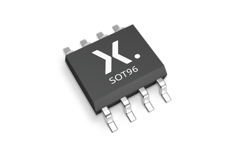
SO8 (SOT96-1) |
SOT96-1 |
SO-SOJ-REFLOW
SO-SOJ-WAVE WAVE_BG-BD-1 |
Not available |
| 74HCT6323AD,118 (935013720118) |
Obsolete | 7T6323A | SOT96-1_118 |
环境信息
下表中的所有产品型号已停产。参见表 停产信息 了解更多信息。
| 型号 | 可订购的器件编号 | 化学成分 | RoHS | RHF指示符 |
|---|---|---|---|---|
| 74HCT6323AD | 74HCT6323AD,112 | 74HCT6323AD |
|
|
| 74HCT6323AD | 74HCT6323AD,118 | 74HCT6323AD |
|
|
Series
文档 (9)
| 文件名称 | 标题 | 类型 | 日期 |
|---|---|---|---|
| 74HC_HCT6323A | Programmable ripple counter with oscillator; 3-state | Data sheet | 2018-07-09 |
| AN11044 | Pin FMEA 74HC/74HCT family | Application note | 2019-01-09 |
| Nexperia_package_poster | Nexperia package poster | Leaflet | 2020-05-15 |
| SO8_SOT96-1_mk | plastic, small outline package; 8 leads; 1.27 mm pitch; 4.9 mm x 3.9 mm x 1.75 mm body | Marcom graphics | 2017-01-28 |
| SOT96-1 | plastic, small outline package; 8 leads; 1.27 mm pitch; 4.9 mm x 3.9 mm x 1.75 mm body | Package information | 2020-04-21 |
| SO-SOJ-REFLOW | Footprint for reflow soldering | Reflow soldering | 2009-10-08 |
| HCT_USER_GUIDE | HC/T User Guide | User manual | 1997-10-31 |
| SO-SOJ-WAVE | Footprint for wave soldering | Wave soldering | 2009-10-08 |
| WAVE_BG-BD-1 | Wave soldering profile | Wave soldering | 2021-09-08 |
支持
如果您需要设计/技术支持,请告知我们并填写 应答表 我们会尽快回复您。
模型
No documents available
PCB Symbol, Footprint and 3D Model
| Model Name | 描述 |
|---|---|
|
|
How does it work?
The interactive datasheets are based on the Nexperia MOSFET precision electrothermal models. With our interactive datasheets you can simply specify your own conditions interactively. Start by changing the values of the conditions. You can do this by using the sliders in the condition fields. By dragging the sliders you will see how the MOSFET will perform at the new conditions set.
74HCT6323AD
Programmable ripple counter with oscillator; 3-state
从安世半导体购买
| SKU | 库存* | MOQ | 单位价格 | 数量 |
|---|