可订购部件
| 型号 | 可订购的器件编号 | 订购代码(12NC) | 封装 | 从经销商处购买 |
|---|---|---|---|---|
| 74AUP2G80GN | 74AUP2G80GN,115 | 935292229115 | SOT1116 | 订单产品 |
Register once, drag and drop ECAD models into your CAD tool and speed up your design.
Click here for more informationLow-power dual D-type flip-flop; positive-edge trigger
74AUP2G80提供双路正沿触发D类触发器。在时钟脉冲从低到高转换时,数据输入处的信息会被传输到Q输出。在时钟从低到高转换前的某个建立时间,输入引脚D必须保持稳定,以进行可预测操作。
所有输入的施密特触发器动作使电路在0.8 V至3.6 V的整个VCC范围内容许较缓慢的输入上升时间和下降时间。
该器件可确保在0.8 V至3.6 V的整个VCC范围内具有极低的静态和动态功耗。
该器件完全指定用于使用IOFF的部分掉电应用。IOFF电路可禁用输出,从而防止掉电时电流回流对器件造成的损坏。
| 型号 | Product status | VCC (V) | Logic switching levels | Output drive capability (mA) | tpd (ns) | fmax (MHz) | Power dissipation considerations | Tamb (°C) | Rth(j-a) (K/W) | Ψth(j-top) (K/W) | Rth(j-c) (K/W) | Package name |
|---|---|---|---|---|---|---|---|---|---|---|---|---|
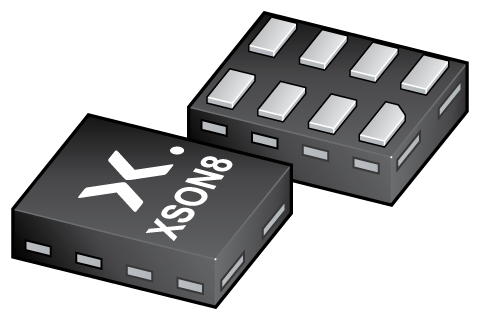
| 74AUP2G80GN | Production | 0.8 - 3.6 | CMOS | ± 1.9 | 9.1 | 400 | ultra low | -40~125 | 238 | 10.6 | 148 | XSON8 |
| Model Name | 描述 |
|---|---|
|
|
| 型号 | 可订购的器件编号,(订购码(12NC)) | 状态 | 标示 | 封装 | 外形图 | 回流焊/波峰焊 | 包装 |
|---|---|---|---|---|---|---|---|
| 74AUP2G80GN | 74AUP2G80GN,115 (935292229115) |
Active | pT |
XSON8 (SOT1116) |
SOT1116 |
REFLOW_BG-BD-1
|
SOT1116_115 |
| 文件名称 | 标题 | 类型 | 日期 |
|---|---|---|---|
| 74AUP2G80 | Low-power dual D-type flip-flop; positive-edge trigger | Data sheet | 2023-07-21 |
| AN11052 | Pin FMEA for AUP family | Application note | 2019-01-09 |
| Nexperia_document_guide_MiniLogic_MicroPak_201808 | MicroPak leadless logic portfolio guide | Brochure | 2018-09-03 |
| SOT1116 | 3D model for products with SOT1116 package | Design support | 2023-02-02 |
| aup2g80 | aup2g80 IBIS model | IBIS model | 2013-04-07 |
| Nexperia_document_leaflet_Logic_AUP_technology_portfolio_201904 | Nexperia_document_leaflet_Logic_AUP_technology_portfolio_201904 | Leaflet | 2019-04-12 |
| Nexperia_package_poster | Nexperia package poster | Leaflet | 2020-05-15 |
| SOT1116 | plastic, leadless extremely thin small outline package; 8 terminals; 0.3 mm pitch; 1.2 mm x 1 mm x 0.35 mm body | Package information | 2022-06-02 |
| SOT1116_115 | XSON8 ; Reel pack for SMD, 7''; Q1/T1 product orientation | Packing information | 2020-04-21 |
| 74AUP2G80GN_Nexperia_Product_Reliability | 74AUP2G80GN Nexperia Product Reliability | Quality document | 2023-05-29 |
| REFLOW_BG-BD-1 | Reflow soldering profile | Reflow soldering | 2021-04-06 |
| MAR_SOT1116 | MAR_SOT1116 Topmark | Top marking | 2013-06-03 |
| 型号 | Orderable part number | Ordering code (12NC) | 状态 | 包装 | Packing Quantity | 在线购买 |
|---|---|---|---|---|---|---|
| 74AUP2G80GN | 74AUP2G80GN,115 | 935292229115 | Active | SOT1116_115 | 5,000 | 订单产品 |
安世半导体客户可通过我们的销售机构或直接通过在线样品商店订购样品: https://extranet.nexperia.com.
样品订单通常需要2-4天寄送时间。
如果您尚未取得安世半导体的直接采购帐号,我们的全球与区域经销网络可以协助您取得样品。
The interactive datasheets are based on the Nexperia MOSFET precision electrothermal models. With our interactive datasheets you can simply specify your own conditions interactively. Start by changing the values of the conditions. You can do this by using the sliders in the condition fields. By dragging the sliders you will see how the MOSFET will perform at the new conditions set.
Low-power dual D-type flip-flop; positive-edge trigger
| SKU | 库存* | MOQ | 单位价格 | 数量 |
|---|