Block diagram
Products - Power
Design challenges
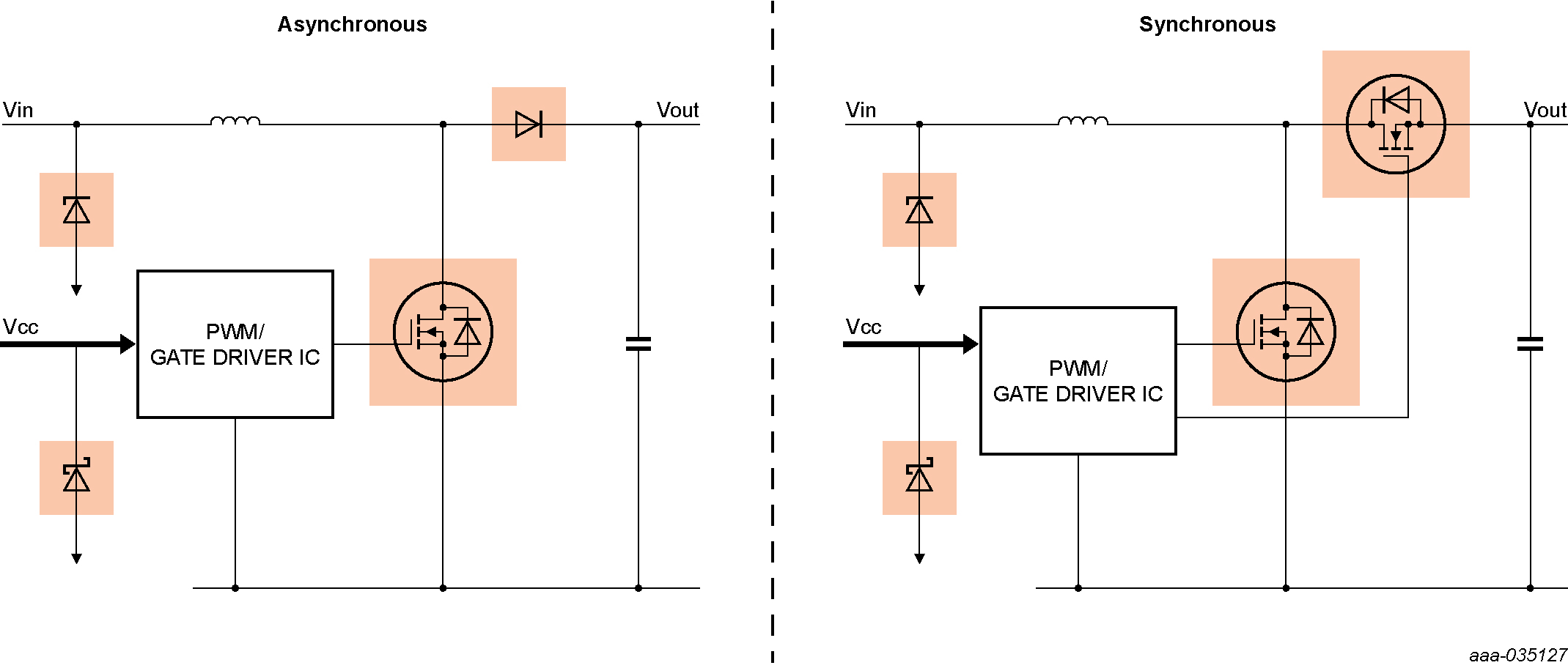
- Point of load non-isolated DC/DC boost converter circuit
- Economical, two-MOSFET design - low QG(tot) and low FOM for best efficiency
- Easily switch from asynchronous to synchronous conversion depending on choice of high-side diode or MOSFET
- Lower switch losses improve thermal behaviour
- LFPAK and CFP (both clip-bond package) allow a high-efficiency DCDC converter solutions, while reducing costs (less heating to dissipate)
- Possibility to go to higher switching frequency (FSW), which leads to smaller inductances and smaller capacitors
- Best thermal performance thanks to clip-bonding package
MOSFET and GaN FET Handbook
Drawing on over 20 years’ of experience, the MOSFET and GaN FET Application Handbook: A Power Design Engineer’s Guide brings together a comprehensive set of learning and reference materials relating to the use of MOSFETs and GaN FETs in real world systems.