
特性
-
Automotive product qualification in accordance with AEC-Q100 (Grade 1)
-
Specified from -40 °C to +85 °C and from -40 °C to +125 °C
-
-
Supply voltage range from 2.3 V to 3.6 V
-
Standard ’126’-type pinout
-
High noise immunity
-
Complies with JEDEC standard:
-
JESD8-5 (2.3 V to 2.7 V)
-
JESD8-B/JESD36 (2.7 V to 3.6 V)
-
-
5 Ω switch connection between two ports
-
Rail to rail switching on data I/O ports
-
CMOS low power consumption
-
Latch-up performance exceeds 250 mA per JESD78B Class I level A
-
IOFF circuitry provides partial Power-down mode operation
-
DHVQFN package with Side-Wettable Flanks enabling Automatic Optical Inspection (AOI) of solder joints
-
ESD protection:
-
HBM: ANSI/ESDA/JEDEC JS-001 class 2 exceeds 2000 V
-
CDM: ANSI/ESDA/JEDEC JS-002 class C3 exceeds 1000 V
-
参数类型
| Type number | Product status | VCC (V) | RON (Ω) | Logic switching levels | tpd (ns) | Power dissipation considerations | Tamb (°C) | Rth(j-a) (K/W) | Ψth(j-top) (K/W) | Rth(j-c) (K/W) | Package name |
|---|---|---|---|---|---|---|---|---|---|---|---|
| 74CBTLV3126BQ-Q100 | Production | 2.3 - 3.6 | 7 | CMOS/LVTTL | 0.2 | very low | -40~125 | 107 | 21.3 | 75 | DHVQFN14 |
| 74CBTLV3126PW-Q100 | Production | 2.3 - 3.6 | 7 | CMOS/LVTTL | 0.2 | very low | -40~125 | 141 | 8.0 | 68 | TSSOP14 |
封装
| 型号 | 封装 | 尺寸版本 | 回流焊/波峰焊 | 包装 | 状态 | 标示 | 可订购的器件编号,(订购码(12NC)) |
|---|---|---|---|---|---|---|---|
| 74CBTLV3126BQ-Q100 | 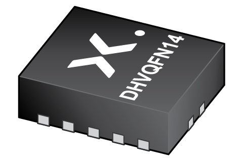 DHVQFN14 (SOT762-1) | SOT762-1 | SOT762-1_115 | Active | V3126 | 74CBTLV3126BQ-Q10X ( 9353 009 57115 ) | |
| 74CBTLV3126PW-Q100 | 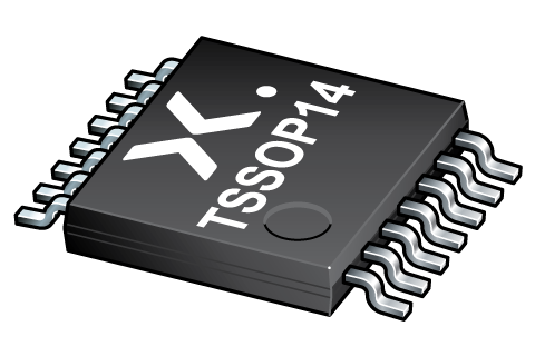 TSSOP14 (SOT402-1) | SOT402-1 | SSOP-TSSOP-VSO-WAVE | SOT402-1_118 | Active | TLV3126 | 74CBTLV3126PW-Q10J ( 9353 009 56118 ) |
环境信息
| 型号 | 可订购的器件编号 | 化学成分 | RoHS | RHF指示符 | 无铅转换日期 |
|---|---|---|---|---|---|
| 74CBTLV3126BQ-Q100 | 74CBTLV3126BQ-Q10X | 74CBTLV3126BQ-Q100 | Always Pb-free | ||
| 74CBTLV3126PW-Q100 | 74CBTLV3126PW-Q10J | 74CBTLV3126PW-Q100 | Always Pb-free |
文档 (6)
| 文件名称 | 标题 | 类型 | 日期 |
|---|---|---|---|
| 74CBTLV3126_Q100 | 4-bit bus switch | Data sheet | 2024-04-11 |
| cbtlv3126 | 74CBTLV3126 IBIS model | IBIS model | 2015-02-22 |
| Nexperia_Selection_guide_2023 | Nexperia Selection Guide 2023 | Selection guide | 2023-05-10 |
| SOT762-1 | plastic, leadless dual in-line compatible thermal enhanced very thin quad flat package; 14 terminals; 0.5 mm pitch; 2.5 x 3 x 1 mm body | Package information | 2023-04-05 |
| SSOP-TSSOP-VSO-WAVE | Footprint for wave soldering | Wave soldering | 2009-10-08 |
| SOT402-1 | plastic, thin shrink small outline package; 14 leads; 0.65 mm pitch; 5 mm x 4.4 mm x 1.2 mm body | Package information | 2023-11-07 |
支持
如果您需要设计/技术支持,请告知我们并填写 应答表, 我们会尽快回复您。
模型
| 文件名称 | 标题 | 类型 | 日期 |
|---|---|---|---|
| cbtlv3126 | 74CBTLV3126 IBIS model | IBIS model | 2015-02-22 |
样品
安世半导体客户可通过我们的销售机构或直接通过在线样品商店订购样品: https://extranet.nexperia.com.
样品订单通常需要2-4天寄送时间。
如果您尚未取得安世半导体的直接采购帐号,我们的全球与区域经销网络可以协助您取得样品。