
特性
-
J and K inputs for easy D-type flip-flop
-
Toggle flip-flop or "do nothing" mode
-
Wide supply voltage range:
-
For 74HC109: from 2.0 V to 6.0 V
-
For 74HCT109: from 4.5 V to 5.5 V
-
-
CMOS low power dissipation
-
High noise immunity
-
Input levels:
-
For 74HC109: CMOS level
-
For 74HCT109: TTL level
-
-
Latch-up performance exceeds 100 mA per JESD 78 Class II Level B
-
74HC109 complies with JEDEC standards:
-
JESD8C (2.7 V to 3.6 V)
-
JESD7A (2.0 V to 6.0 V)
-
-
74HCT109 complies with JEDEC standard JESD7A (2.0 V to 6.0 V)
-
ESD protection:
-
HBM: ANSI/ESDA/JEDEC JS-001 class 2 exceeds 2000 V
-
CDM: ANSI/ESDA/JEDEC JS-002 class C3 exceeds 1000 V
-
-
Specified from -40 °C to +85 °C and from -40 °C to +125 °C
参数类型
| Type number | Product status | VCC (V) | Logic switching levels | Output drive capability (mA) | tpd (ns) | fmax (MHz) | Power dissipation considerations | Tamb (°C) | Rth(j-a) (K/W) | Ψth(j-top) (K/W) | Rth(j-c) (K/W) | Package name |
|---|---|---|---|---|---|---|---|---|---|---|---|---|
| 74HC109D | Production | 2.0 - 6.0 | CMOS | ± 5.2 | 15 | 75 | low | -40~125 | 86 | 6.6 | 44 | SO16 |
| 74HC109PW | Production | 2.0 - 6.0 | CMOS | ± 5.2 | 15 | 75 | low | -40~125 | 119 | 3.2 | 48.1 | TSSOP16 |
| 74HCT109D | Production | 4.5 - 5.5 | TTL | ± 4 | 17 | 61 | low | -40~125 | 86 | 6.6 | 44 | SO16 |
| 74HCT109PW | Production | 4.5 - 5.5 | TTL | ± 4 | 17 | 61 | low | -40~125 | 119 | 3.2 | 48.1 | TSSOP16 |
封装
| 型号 | 封装 | 尺寸版本 | 回流焊/波峰焊 | 包装 | 状态 | 标示 | 可订购的器件编号,(订购码(12NC)) |
|---|---|---|---|---|---|---|---|
| 74HC109D | 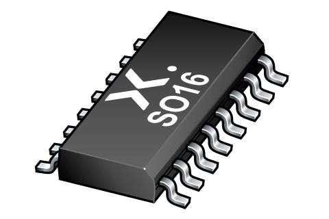 SO16 (SOT109-1) | SOT109-1 | SO-SOJ-REFLOW SO-SOJ-WAVE | SOT109-1_653 | Active | 74HC109D | 74HC109D,653 ( 9337 144 80653 ) |
| 74HC109PW | 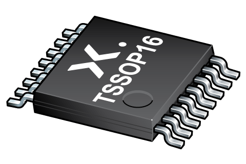 TSSOP16 (SOT403-1) | SOT403-1 | SSOP-TSSOP-VSO-WAVE | SOT403-1_118 | Active | 74HC109 | 74HC109PWJ ( 9356 912 05118 ) |
| 74HCT109D | SO16 (SOT109-1) | SOT109-1 | SO-SOJ-REFLOW SO-SOJ-WAVE | SOT109-1_653 | Active | 74HCT109D | 74HCT109D,653 ( 9337 149 60653 ) |
| 74HCT109PW | TSSOP16 (SOT403-1) | SOT403-1 | SSOP-TSSOP-VSO-WAVE | SOT403-1_118 | Active | HCT109 | 74HCT109PW,118 ( 9351 863 30118 ) |
停产信息
| 型号 | 可订购的器件编号,(订购码(12NC)) | 最后一次购买日期 | 最后一次交货日期 | 替代产品 | 状态 | 备注 |
|---|---|---|---|---|---|---|
| 74HC109D | 933714480652 | 2021-12-31 | 2022-06-30 | 74HC109D | ||
| 74HCT109D | 933714960652 | 2021-12-31 | 2022-06-30 | 74HCT109D | ||
| 74HCT109PW | 935186330112 | 2021-12-31 | 2022-06-30 | 74HCT109PW |
环境信息
| 型号 | 可订购的器件编号 | 化学成分 | RoHS | RHF指示符 | 无铅转换日期 |
|---|---|---|---|---|---|
| 74HC109D | 74HC109D,653 | 74HC109D | week 6, 2004 | ||
| 74HC109PW | 74HC109PWJ | 74HC109PW | |||
| 74HCT109D | 74HCT109D,653 | 74HCT109D | week 6, 2004 | ||
| 74HCT109PW | 74HCT109PW,118 | 74HCT109PW | week 10, 2005 |
文档 (9)
| 文件名称 | 标题 | 类型 | 日期 |
|---|---|---|---|
| 74HC_HCT109 | Dual JK flip-flop with set and reset; positive-edge-trigger | Data sheet | 2024-02-21 |
| AN11044 | Pin FMEA 74HC/74HCT family | Application note | 2019-01-09 |
| HCT_USER_GUIDE | HC/T User Guide | User manual | 1997-10-31 |
| SO-SOJ-WAVE | Footprint for wave soldering | Wave soldering | 2009-10-08 |
| SO-SOJ-REFLOW | Footprint for reflow soldering | Reflow soldering | 2009-10-08 |
| WAVE_BG-BD-1 | Wave soldering profile | Wave soldering | 2021-09-08 |
| SOT109-1 | plastic, small outline package; 16 leads; 1.27 mm pitch; 9.9 mm x 3.9 mm x 1.75 mm body | Package information | 2023-11-07 |
| SOT403-1 | plastic, thin shrink small outline package; 16 leads; 5 mm x 4.4 mm x 1.2 mm body | Package information | 2023-11-08 |
| SSOP-TSSOP-VSO-WAVE | Footprint for wave soldering | Wave soldering | 2009-10-08 |
支持
如果您需要设计/技术支持,请告知我们并填写 应答表, 我们会尽快回复您。
样品
安世半导体客户可通过我们的销售机构或直接通过在线样品商店订购样品: https://extranet.nexperia.com.
样品订单通常需要2-4天寄送时间。
如果您尚未取得安世半导体的直接采购帐号,我们的全球与区域经销网络可以协助您取得样品。