
特性
-
Wide supply voltage range:
-
VCC(A): 0.8 V to 3.6 V
-
VCC(B): 0.8 V to 3.6 V
-
-
Complies with JEDEC standards:
-
JESD8-12 (0.8 V to 1.3 V)
-
JESD8-11 (0.9 V to 1.65 V)
-
JESD8-7 (1.2 V to 1.95 V)
-
JESD8-5 (1.8 V to 2.7 V)
-
JESD8-B (2.7 V to 3.6 V)
-
-
ESD protection:
-
HBM: ANSI/ESDA/Jedec JS-001 Class 3B exceeds 8000 V
-
CDM: ANSI/ESDA/Jedec JS-002 Class C3 exceeds 1500 V
-
-
Maximum data rates:
-
380 Mbit/s (≥ 1.8 V to 3.3 V translation)
-
200 Mbit/s (≥ 1.1 V to 3.3 V translation)
-
200 Mbit/s (≥ 1.1 V to 2.5 V translation)
-
200 Mbit/s (≥ 1.1 V to 1.8 V translation)
-
150 Mbit/s (≥ 1.1 V to 1.5 V translation)
-
100 Mbit/s (≥ 1.1 V to 1.2 V translation)
-
-
Suspend mode
-
Latch-up performance exceeds 100 mA per JESD 78 Class II
-
Inputs accept voltages up to 3.6 V
-
IOFF circuitry provides partial Power-down mode operation
-
Specified from -40 °C to +85 °C and -40 °C to +125 °C
参数类型
| Type number | Product status | VCC(A) (V) | VCC(B) (V) | Logic switching levels | Output drive capability (mA) | tpd (ns) | Nr of bits | Power dissipation considerations | Tamb (°C) | Rth(j-a) (K/W) | Ψth(j-top) (K/W) | Rth(j-c) (K/W) | Package name |
|---|---|---|---|---|---|---|---|---|---|---|---|---|---|
| 74AVC4T774BQ | Production | 0.8 - 3.6 | 0.8 - 3.6 | CMOS/LVTTL | ± 12 | 2.1 | 4 | very low | -40~125 | 92 | 13.0 | 61 | DHVQFN16 |
| 74AVC4T774GU | Production | 0.8 - 3.6 | 0.8 - 3.6 | CMOS/LVTTL | ± 12 | 2.1 | 4 | very low | -40~125 | 99 | 4.1 | 87 | XQFN16 |
封装
| 型号 | 封装 | 尺寸版本 | 回流焊/波峰焊 | 包装 | 状态 | 标示 | 可订购的器件编号,(订购码(12NC)) |
|---|---|---|---|---|---|---|---|
| 74AVC4T774BQ | 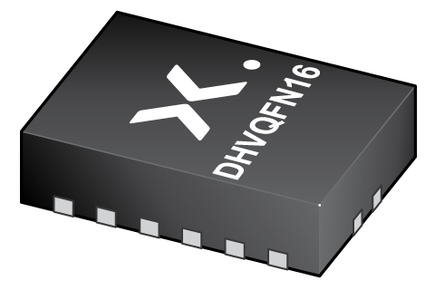 DHVQFN16 (SOT763-1) | SOT763-1 | SOT763-1_115 | Active | C4T774 | 74AVC4T774BQX ( 9353 413 26115 ) | |
| 74AVC4T774GU | 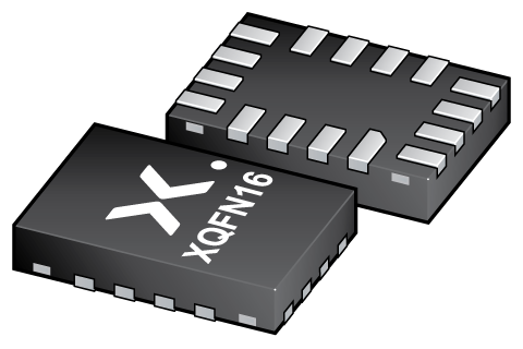 XQFN16 (SOT1161-1) | SOT1161-1 | SOT1161-1_184 | Active | Standard Marking | 74AVC4T774GUZ ( 9353 413 27184 ) | |
| SOT1161-1_115 | Active | Standard Marking | 74AVC4T774GUX ( 9353 413 27115 ) |
环境信息
| 型号 | 可订购的器件编号 | 化学成分 | RoHS | RHF指示符 | 无铅转换日期 |
|---|---|---|---|---|---|
| 74AVC4T774BQ | 74AVC4T774BQX | 74AVC4T774BQ | week 25, 2019 | ||
| 74AVC4T774GU | 74AVC4T774GUZ | 74AVC4T774GU | |||
| 74AVC4T774GU | 74AVC4T774GUX | 74AVC4T774GU | week 25, 2019 |
文档 (6)
| 文件名称 | 标题 | 类型 | 日期 |
|---|---|---|---|
| 74AVC4T774 | 4-bit dual supply translating transceiver; 3-state | Data sheet | 2023-01-02 |
| Nexperia_document_guide_Logic_translators | Nexperia Logic Translators | Brochure | 2021-04-12 |
| avc4t774 | AVC4T774 IBIS model | IBIS model | 2017-10-04 |
| Nexperia_Selection_guide_2023 | Nexperia Selection Guide 2023 | Selection guide | 2023-05-10 |
| SOT763-1 | plastic, leadless dual in-line compatible thermal enhanced very thin quad flat package; 16 terminals; 0.5 mm pitch; 3.5 mm x 2.5 mm x 1 mm body | Package information | 2023-05-11 |
| SOT1161-1 | plastic, leadless extermely thin quad flat package; 16 terminals; 0.4 mm pitch; 2.6 mm x 1.8 mm x 0.5 mm body | Package information | 2022-06-15 |
订购、定价与供货
样品
安世半导体客户可通过我们的销售机构或直接通过在线样品商店订购样品: https://extranet.nexperia.com.
样品订单通常需要2-4天寄送时间。
如果您尚未取得安世半导体的直接采购帐号,我们的全球与区域经销网络可以协助您取得样品。