
特性
-
Wide supply voltage range:
-
VCC(A): 1.65 V to 3.6 V and VCC(B): 2.3 V to 5.5 V
-
-
Maximum data rates:
-
Push-pull: 24 Mbps
-
-
IOFF circuitry provides partial Power-down mode operation
-
Inputs accept voltages up to 5.5 V
-
ESD protection:
-
HBM: ANSI/ESDA/JEDEC JS-001 class 2 exceeds 2500 V for A port
-
HBM: ANSI/ESDA/JEDEC JS-001 class 3B exceeds 8000 V for B port
-
CDM: ANSI/ESDA/JEDEC JS-002 class C3 exceeds 1500 V
-
-
Latch-up performance exceeds 100 mA per JESD 78B Class II
-
Multiple package options
-
Specified from -40 °C to +85 °C and -40 °C to +125 °C
目标应用
-
Desktop PC
-
Handset
-
Smartphone
-
Tablet
参数类型
| Type number | Product status | VCC(A) (V) | VCC(B) (V) | Logic switching levels | Output drive capability (mA) | tpd (ns) | Nr of bits | Power dissipation considerations | Tamb (°C) | Rth(j-a) (K/W) | Ψth(j-top) (K/W) | Rth(j-c) (K/W) | Package name |
|---|---|---|---|---|---|---|---|---|---|---|---|---|---|
| NXS0101GM | Production | 1.2 - 3.6 | 2.3 - 5.5 | CMOS | - 0.02 / 1.0 | 4.7 | 1 | low | -40~125 | 253 | 4.5 | 123 | XSON6 |
| NXS0101GS | Production | 1.2 - 3.6 | 2.3 - 5.5 | CMOS | - 0.02 / 1.0 | 4.7 | 1 | low | -40~125 | - | - | - | XSON6 |
| NXS0101GW | Production | 1.65 - 3.6 | 2.3 - 5.5 | CMOS | - 0.02 / 1.0 | 4.7 | 1 | low | -40~125 | - | - | - | TSSOP6 |
封装
| 型号 | 封装 | 尺寸版本 | 回流焊/波峰焊 | 包装 | 状态 | 标示 | 可订购的器件编号,(订购码(12NC)) |
|---|---|---|---|---|---|---|---|
| NXS0101GM |  XSON6 (SOT886) | SOT886 | REFLOW_BG-BD-1 | SOT886_115 | Active | m1 | NXS0101GMX ( 9352 897 22115 ) |
| NXS0101GS |  XSON6 (SOT1202) | SOT1202 | REFLOW_BG-BD-1 | SOT1202_125 | Active | m1 | NXS0101GSH ( 9356 908 98125 ) |
| NXS0101GW | 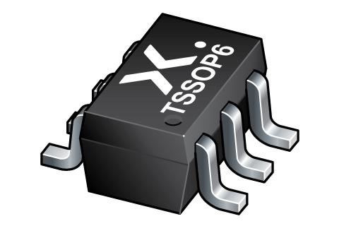 TSSOP6 (SOT363-2) | SOT363-2 | SOT363-2_125 | Active | m1 | NXS0101GWH ( 9352 897 24125 ) |
环境信息
| 型号 | 可订购的器件编号 | 化学成分 | RoHS | RHF指示符 | 无铅转换日期 |
|---|---|---|---|---|---|
| NXS0101GM | NXS0101GMX | NXS0101GM | |||
| NXS0101GS | NXS0101GSH | NXS0101GS | |||
| NXS0101GW | NXS0101GWH | NXS0101GW |
文档 (10)
| 文件名称 | 标题 | 类型 | 日期 |
|---|---|---|---|
| NXS0101 | Dual supply translating transceiver; open drain; auto direction sensing | Data sheet | 2023-11-16 |
| NXS0101_Q100 | Dual supply translating transceiver; open drain; auto direction sensing | Data sheet | 2023-11-16 |
| nxs0101 | NXS0101 IBIS model | IBIS model | 2020-11-05 |
| MAR_SOT1202 | MAR_SOT1202 Topmark | Top marking | 2013-06-03 |
| SOT1202 | plastic, leadless extremely thin small outline package; 6 terminals; 0.35 mm pitch; 1 mm x 1mm x 0.35 mm body | Package information | 2022-06-01 |
| REFLOW_BG-BD-1 | Reflow soldering profile | Reflow soldering | 2021-04-06 |
| SOT363-2 | plastic thin shrink small outline package; 6 leads; body width 1.25 mm | Package information | 2022-11-21 |
| MAR_SOT886 | MAR_SOT886 Topmark | Top marking | 2013-06-03 |
| SOT886 | plastic, leadless extremely thin small outline package; 6 terminals; 0.5 mm pitch; 1 mm x 1.45 mm x 0.5 mm body | Package information | 2022-06-01 |
| REFLOW_BG-BD-1 | Reflow soldering profile | Reflow soldering | 2021-04-06 |
样品
安世半导体客户可通过我们的销售机构或直接通过在线样品商店订购样品: https://extranet.nexperia.com.
样品订单通常需要2-4天寄送时间。
如果您尚未取得安世半导体的直接采购帐号,我们的全球与区域经销网络可以协助您取得样品。