
特性
-
Automotive product qualification in accordance with AEC-Q100 (Grade 1)
-
Specified from -40 °C to +85 °C and from -40 °C to +125 °C
-
-
Wide supply voltage range from 1.2 V to 3.6 V
-
Overvoltage tolerant inputs to 5.5 V
-
CMOS low power consumption
-
Direct interface with TTL levels
-
Output drive capability 50 Ω transmission lines at +85 °C
-
Complies with JEDEC standard:
-
JESD8-7A (1.65 V to 1.95 V)
-
JESD8-5A (2.3 V to 2.7 V)
-
JESD8-C/JESD36 (2.7 V to 3.6 V)
-
-
ESD protection:
-
HBM: ANSI/ESDA/JEDEC JS-001 class 2 exceeds 2000 V
-
CDM: ANSI/ESDA/JEDEC JS-002 class C3 exceeds 1000 V
-
-
DHVQFN package with Side-Wettable Flanks enabling Automatic Optical Inspection (AOI) of solder joints
参数类型
| Type number | Product status | VCC (V) | Logic switching levels | Output drive capability (mA) | tpd (ns) | fmax (MHz) | Power dissipation considerations | Tamb (°C) | Rth(j-a) (K/W) | Ψth(j-top) (K/W) | Rth(j-c) (K/W) | Package name |
|---|---|---|---|---|---|---|---|---|---|---|---|---|
| 74LVC273BQ-Q100 | Production | 1.2 - 3.6 | CMOS/LVTTL | ± 24 | 6 | 230 | low | -40~125 | 79 | 9.6 | 50 | DHVQFN20 |
| 74LVC273D-Q100 | Production | 1.2 - 3.6 | CMOS/LVTTL | ± 24 | 6 | 230 | low | -40~125 | 85 | 27.7 | 61 | SO20 |
| 74LVC273PW-Q100 | Production | 1.2 - 3.6 | CMOS/LVTTL | ± 24 | 6 | 230 | low | -40~125 | 101 | 4.7 | 45 | TSSOP20 |
封装
| 型号 | 封装 | 尺寸版本 | 回流焊/波峰焊 | 包装 | 状态 | 标示 | 可订购的器件编号,(订购码(12NC)) |
|---|---|---|---|---|---|---|---|
| 74LVC273BQ-Q100 | 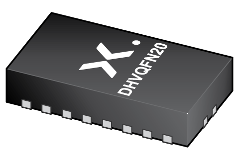 DHVQFN20 (SOT764-1) | SOT764-1 | SOT764-1_115 | Active | LVC273 | 74LVC273BQ-Q100X ( 9353 024 59115 ) | |
| 74LVC273D-Q100 | 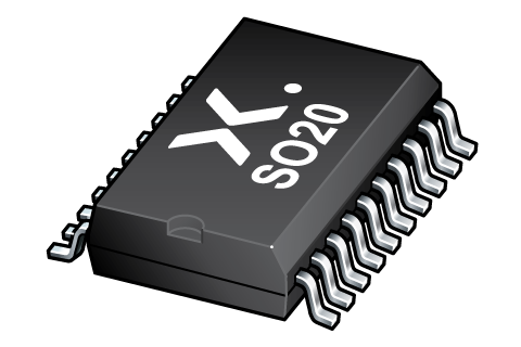 SO20 (SOT163-1) | SOT163-1 | WAVE_BG-BD-1 | SOT163-1_118 | Active | 74LVC273D | 74LVC273D-Q100J ( 9353 024 61118 ) |
| 74LVC273PW-Q100 | 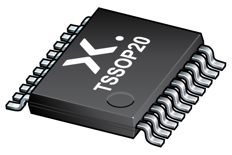 TSSOP20 (SOT360-1) | SOT360-1 | SSOP-TSSOP-VSO-WAVE | SOT360-1_118 | Active | LVC273 | 74LVC273PW-Q100J ( 9353 024 62118 ) |
环境信息
| 型号 | 可订购的器件编号 | 化学成分 | RoHS | RHF指示符 | 无铅转换日期 |
|---|---|---|---|---|---|
| 74LVC273BQ-Q100 | 74LVC273BQ-Q100X | 74LVC273BQ-Q100 | Always Pb-free | ||
| 74LVC273D-Q100 | 74LVC273D-Q100J | 74LVC273D-Q100 | Always Pb-free | ||
| 74LVC273PW-Q100 | 74LVC273PW-Q100J | 74LVC273PW-Q100 | Always Pb-free |
文档 (11)
| 文件名称 | 标题 | 类型 | 日期 |
|---|---|---|---|
| 74LVC273_Q100 | Octal D-type flip-flop with reset; positive-edge trigger | Data sheet | 2023-08-25 |
| AN263 | Power considerations when using CMOS and BiCMOS logic devices | Application note | 2023-02-07 |
| AN11009 | Pin FMEA for LVC family | Application note | 2019-01-09 |
| lvc273 | lvc273 IBIS model | IBIS model | 2013-04-07 |
| Nexperia_Selection_guide_2023 | Nexperia Selection Guide 2023 | Selection guide | 2023-05-10 |
| lvc | lvc Spice model | SPICE model | 2013-05-06 |
| SOT764-1 | plastic, leadless dual in-line compatible thermal enhanced very thin quad flat package; 20 terminals; 0.5 mm pitch; 4.5 mm x 2.5 mm x 1 mm body | Package information | 2022-06-21 |
| SSOP-TSSOP-VSO-WAVE | Footprint for wave soldering | Wave soldering | 2009-10-08 |
| SOT360-1 | plastic, thin shrink small outline package; 20 leads; 0.65 mm pitch; 6.5 mm x 4.4 mm x 1.1 mm body | Package information | 2022-06-21 |
| SOT163-1 | plastic, small outline package; 20 leads; 1.27 mm pitch; 12.8 mm x 7.5 mm x 2.65 mm body | Package information | 2022-06-20 |
| WAVE_BG-BD-1 | Wave soldering profile | Wave soldering | 2021-09-08 |
支持
如果您需要设计/技术支持,请告知我们并填写 应答表, 我们会尽快回复您。
样品
安世半导体客户可通过我们的销售机构或直接通过在线样品商店订购样品: https://extranet.nexperia.com.
样品订单通常需要2-4天寄送时间。
如果您尚未取得安世半导体的直接采购帐号,我们的全球与区域经销网络可以协助您取得样品。