
Register once, drag and drop ECAD models into your CAD tool and speed up your design.
Click here for more information74AUP1G79GF
74AUP1G79提供单路正沿触发D类触发器。数据输入处的信息会在时钟脉冲从低到高转换时被传输到Q输出。在时钟从低到高转换前的某个建立时间,D输入必须保持稳定,以进行可预测操作。
所有输入的施密特触发器动作使电路在0.8 V至3.6 V的整个VCC范围内容许较缓慢的输入上升时间和下降时间。
该器件可确保在0.8 V至3.6 V的整个VCC范围内具有极低的静态和动态功耗。
该器件完全指定用于使用IOFF的部分掉电应用。IOFF电路可禁用输出,从而防止掉电时电流回流对器件造成的损坏。
Features and benefits
- 0.8 V至3.6 V的宽电源电压范围
- 高抗噪性
- 符合JEDEC标准:
- JESD8-12(0.8 V至1.3 V)
- JESD8-11(0.9 V至1.65 V)
- JESD8-7(1.2 V至1.95 V)
- JESD8-5(1.8 V至2.7 V)
- JESD8-B(2.7 V至3.6 V)
- ESD保护:
- HBM JESD22-A114F 3A类超过5000 V
- MM JESD22-A115-A超过200 V
- CDM JESD22-C101-E超过1000 V
- 低静态功耗;ICC = 0.9 μA(最大值)
- 根据JESD 78 II类,锁存性能超过100 mA
- 输入接受高达3.6 V的电压
- 低噪声过冲和欠冲<VCC的10 %
- IOFF电路提供部分掉电模式操作
- 多个封装选项
- 指定温度范围为-40 °C至+85 °C和-40 °C至+125 °C
参数类型
| 型号 | Product status | Package name |
|---|---|---|
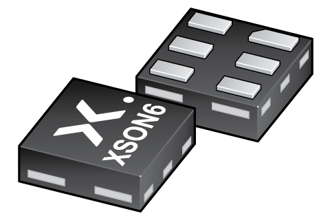
| 74AUP1G79GF | End of life | XSON6 |
PCB Symbol, Footprint and 3D Model
| Model Name | 描述 |
|---|---|
|
|
封装
下表中的所有产品型号已停产。参见表 停产信息 了解更多信息。
| 型号 | 可订购的器件编号,(订购码(12NC)) | 状态 | 标示 | 封装 | 外形图 | 回流焊/波峰焊 | 包装 |
|---|---|---|---|---|---|---|---|
| 74AUP1G79GF | 74AUP1G79GF,132 (935281117132) |
Obsolete | pP |
XSON6 (SOT891) |
SOT891 |
REFLOW_BG-BD-1
|
SOT891_132 |
环境信息
下表中的所有产品型号已停产。参见表 停产信息 了解更多信息。
| 型号 | 可订购的器件编号 | 化学成分 | RoHS | RHF指示符 |
|---|---|---|---|---|
| 74AUP1G79GF | 74AUP1G79GF,132 | 74AUP1G79GF |
|
|
Series
文档 (12)
| 文件名称 | 标题 | 类型 | 日期 |
|---|---|---|---|
| 74AUP1G79 | Low-power D-type flip-flop; positive-edge trigger | Data sheet | 2023-07-24 |
| AN10161 | PicoGate Logic footprints | Application note | 2002-10-29 |
| AN11052 | Pin FMEA for AUP family | Application note | 2019-01-09 |
| Nexperia_document_guide_MiniLogic_MicroPak_201808 | MicroPak leadless logic portfolio guide | Brochure | 2018-09-03 |
| SOT891 | 3D model for products with SOT891 package | Design support | 2019-10-03 |
| aup1g79 | 74AUP1G79 IBIS model | IBIS model | 2014-12-14 |
| Nexperia_document_leaflet_Logic_AUP_technology_portfolio_201904 | Nexperia_document_leaflet_Logic_AUP_technology_portfolio_201904 | Leaflet | 2019-04-12 |
| Nexperia_package_poster | Nexperia package poster | Leaflet | 2020-05-15 |
| DFN1010-6_SOT891_mk | plastic, extremely thin small outline package; 6 terminals; 0.55 mm pitch; 1 mm x 1 mm x 0.5 mm body | Marcom graphics | 2017-01-28 |
| SOT891 | plastic, leadless extremely thin small outline package; 6 terminals; 0.35 mm pitch; 1 mm x 1 mm x 0.5 mm body | Package information | 2020-04-21 |
| REFLOW_BG-BD-1 | Reflow soldering profile | Reflow soldering | 2021-04-06 |
| MAR_SOT891 | MAR_SOT891 Topmark | Top marking | 2013-06-03 |
How does it work?
The interactive datasheets are based on the Nexperia MOSFET precision electrothermal models. With our interactive datasheets you can simply specify your own conditions interactively. Start by changing the values of the conditions. You can do this by using the sliders in the condition fields. By dragging the sliders you will see how the MOSFET will perform at the new conditions set.
74AUP1G79GF
从安世半导体购买
| SKU | 库存* | MOQ | 单位价格 | 数量 |
|---|