可订购部件
| 型号 | 可订购的器件编号 | 订购代码(12NC) | 封装 | 从经销商处购买 |
|---|---|---|---|---|
| 74LVCH162374ADGG | 74LVCH162374ADGG:1 | 935238770118 | SOT362-1 | 订单产品 |
Register once, drag and drop ECAD models into your CAD tool and speed up your design.
Click here for more information16-bit edge-triggered D-type flip-flop with 30 Ohm series termination resistors; 5 V input/output tolerant; 3-state
The 74LVCH162374A is a 16-bit edge triggered flip-flop featuring separate D-type inputs for each flip-flop and 3-state outputs for bus-oriented applications. The device consists of two sections of 8 edge-triggered flip-flops. A clock (CP) input and an output enable (OE) are provided for each octal. Inputs can be driven from either 3.3 V or 5 V devices. When disabled, up to 5.5 V can be applied to the outputs. These features allow the use of these devices in mixed 3.3 V and 5 V applications. The flip-flops store the state of their individual D-inputs that meet the set-up and hold time requirements on the LOW to HIGH CP transition. When OE is LOW, the contents of the flip-flops are available at the outputs. When OE is HIGH, the outputs go to the high-impedance OFF-state. Operation of the OE input does not affect the state of the flip-flops.
Bus hold on data inputs eliminates the need for external pull-up resistors to hold unused inputs.
To reduce line noise, 30 Ω series termination resistors are included in both high and low output stages.
5 V tolerant inputs/outputs for interfacing with 5 V logic
Wide supply voltage range from 1.2 V to 3.6 V
CMOS low power consumption
Multibyte flow-through standard pinout architecture
Multiple low inductance supply pins for minimum noise and ground bounce
Direct interface with TTL levels
All data inputs have bus hold
High-impedance outputs when VCC = 0 V
Complies with JEDEC standard:
JESD8-7A (1.65 V to 1.95 V)
JESD8-5A (2.3 V to 2.7 V)
JESD8-C/JESD36 (2.7 V to 3.6 V)
ESD protection:
HBM: ANSI/ESDA/JEDEC JS-001 class 2 exceeds 2000 V
CDM: ANSI/ESDA/JEDEC JS-002 class C3 exceeds 1000 V
Specified from -40 °C to +85 °C and -40 °C to +125 °C
| 型号 | Product status | VCC (V) | Logic switching levels | Output drive capability (mA) | tpd (ns) | fmax (MHz) | Power dissipation considerations | Tamb (°C) | Rth(j-a) (K/W) | Ψth(j-top) (K/W) | Rth(j-c) (K/W) | Package name |
|---|---|---|---|---|---|---|---|---|---|---|---|---|
| 74LVCH162374ADGG | Production | 1.2 - 3.6 | CMOS/LVTTL | ± 24 | 3.8 | 150 | low | -40~125 | 82 | 2.0 | 37 | TSSOP48 |
| Model Name | 描述 |
|---|---|
|
|
| 型号 | 可订购的器件编号,(订购码(12NC)) | 状态 | 标示 | 封装 | 外形图 | 回流焊/波峰焊 | 包装 |
|---|---|---|---|---|---|---|---|
| 74LVCH162374ADGG | 74LVCH162374ADGG:1 (935238770118) |
Active | LVCH162374A |
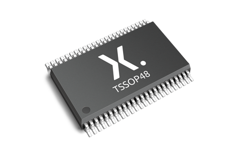
TSSOP48 (SOT362-1) |
SOT362-1 |
SSOP-TSSOP-VSO-WAVE
|
SOT362-1_118 |
| 文件名称 | 标题 | 类型 | 日期 |
|---|---|---|---|
| 74LVCH162374A | 16-bit edge-triggered D-type flip-flop with 30 Ohm series termination resistors; 5 V input/output tolerant; 3-state | Data sheet | 2024-01-31 |
| AN11009 | Pin FMEA for LVC family | Application note | 2019-01-09 |
| AN263 | Power considerations when using CMOS and BiCMOS logic devices | Application note | 2023-02-07 |
| SOT362-1 | 3D model for products with SOT362-1 package | Design support | 2020-01-22 |
| lvch162374a | lvch162374a IBIS model | IBIS model | 2013-04-07 |
| Nexperia_package_poster | Nexperia package poster | Leaflet | 2020-05-15 |
| TSSOP48_SOT362-1_mk | plastic, thin shrink small outline package; 48 leads; 0.5 mm pitch; 12.8 mm x 6.1 mm x 1.2 mm body | Marcom graphics | 2017-01-28 |
| SOT362-1 | plastic thin shrink small outline package; 48 leads; body width 6.1 mm | Package information | 2024-01-05 |
| SOT362-1_118 | TSSOP48; Reel pack for SMD, 13''; Q1/T1 product orientation | Packing information | 2020-04-21 |
| 74LVCH162374ADGG_Nexperia_Product_Reliability | 74LVCH162374ADGG Nexperia Product Reliability | Quality document | 2023-05-29 |
| SSOP-TSSOP-VSO-WAVE | Footprint for wave soldering | Wave soldering | 2009-10-08 |
如果您需要设计/技术支持,请告知我们并填写 应答表 我们会尽快回复您。
| 文件名称 | 标题 | 类型 | 日期 |
|---|---|---|---|
| lvch162374a | lvch162374a IBIS model | IBIS model | 2013-04-07 |
| SOT362-1 | 3D model for products with SOT362-1 package | Design support | 2020-01-22 |
| Model Name | 描述 |
|---|---|
|
|
| 型号 | Orderable part number | Ordering code (12NC) | 状态 | 包装 | Packing Quantity | 在线购买 |
|---|---|---|---|---|---|---|
| 74LVCH162374ADGG | 74LVCH162374ADGG:1 | 935238770118 | Active | SOT362-1_118 | 2,000 | 订单产品 |
安世半导体客户可通过我们的销售机构或直接通过在线样品商店订购样品: https://extranet.nexperia.com.
样品订单通常需要2-4天寄送时间。
如果您尚未取得安世半导体的直接采购帐号,我们的全球与区域经销网络可以协助您取得样品。
The interactive datasheets are based on the Nexperia MOSFET precision electrothermal models. With our interactive datasheets you can simply specify your own conditions interactively. Start by changing the values of the conditions. You can do this by using the sliders in the condition fields. By dragging the sliders you will see how the MOSFET will perform at the new conditions set.
16-bit edge-triggered D-type flip-flop with 30 Ohm series termination resistors; 5 V input/output tolerant; 3-state
| SKU | 库存* | MOQ | 单位价格 | 数量 |
|---|