
Register once, drag and drop ECAD models into your CAD tool and speed up your design.
Click here for more information74LVC373ADB
Octal D-type transparent latch with 5 V tolerant inputs/outputs; 3-state
74LVC373A由八个D型穿透锁存器组成,具有适用于每个锁存器的单独D型输入和适合总线应用的3态真正输出。锁存使能输入(针脚LE)和输出使能输入(针脚OE)为所有内部锁存器共用。
针脚LE为高电平时,D输入(针脚D0至D7)处的数据会输入锁存器。在这种情况下,锁存器是穿透的,即每当与锁存输出对应的D输入发生变化时,锁存输出就会随之变化。针脚LE为低电平时,锁存器存储针脚LE从高电平跃迁至低电平前的一个设置时间在D输入处出现的信息。
针脚OE为低电平时,八个锁存器的内容可在Q输出(针脚Q0至Q7)上获取。针脚OE为高电平时,输出转为高阻抗关断状态。输入引脚OE的操作不会影响锁存器的状态。
输入可通过3.3 V或5 V器件进行驱动。禁用时,可以向输出施加高达5.5 V的电压。这些特性允许将这些器件用作混合3.3 V和5 V应用中的转换器。
74LVC373A在功能上等同于74LVC573A,但针脚排列不同。
Features and benefits
- 5 V容压输入/输出,可实现与5 V逻辑的接合
- 1.2至3.6 V的宽电源电压范围
- CMOS低功耗
- 具有TTL电平的直接接口
- VCC = 0 V时的高阻抗输出
- 符合JEDEC标准:
- JESD8-7A(1.65 V至1.95 V)
- JESD8-5A(2.3 V至2.7 V)
- JESD8-C/JESD36(2.7 V至3.6 V)
- ESD保护:
- HBM JESD22-A114F超过2000 V
- MM JESD22-A115-B超过200 V
- CDM JESD22-C101E超过1000 V
- 额定温度范围为-40 °C至+85 °C和-40 °C至+125 °C
参数类型
| 型号 | Product status | Package name |
|---|---|---|
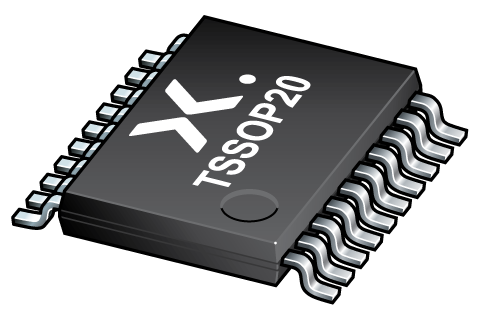
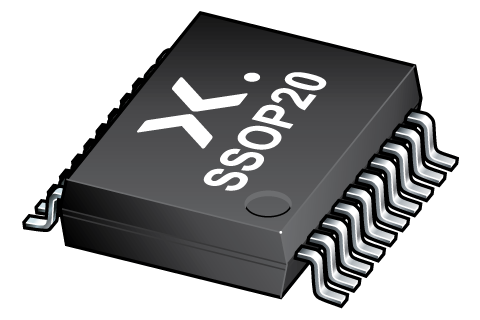
| 74LVC373ADB | End of life | SSOP20 |
PCB Symbol, Footprint and 3D Model
| Model Name | 描述 |
|---|---|
|
|
封装
下表中的所有产品型号已停产。参见表 停产信息 了解更多信息。
| 型号 | 可订购的器件编号,(订购码(12NC)) | 状态 | 标示 | 封装 | 外形图 | 回流焊/波峰焊 | 包装 |
|---|---|---|---|---|---|---|---|
| 74LVC373ADB | 74LVC373ADB,112 (935218640112) |
Withdrawn / End-of-life | LVC373A |
SSOP20 (SOT339-1) |
SOT339-1 |
SSOP-TSSOP-VSO-WAVE
|
Not available |
| 74LVC373ADB,118 (935218640118) |
Obsolete | LVC373A | SOT339-1_118 |
环境信息
下表中的所有产品型号已停产。参见表 停产信息 了解更多信息。
| 型号 | 可订购的器件编号 | 化学成分 | RoHS | RHF指示符 |
|---|---|---|---|---|
| 74LVC373ADB | 74LVC373ADB,112 | 74LVC373ADB |
|
|
| 74LVC373ADB | 74LVC373ADB,118 | 74LVC373ADB |
|
|
文档 (8)
| 文件名称 | 标题 | 类型 | 日期 |
|---|---|---|---|
| 74LVC373A | Octal D-type transparent latch with 5 V tolerant inputs/outputs; 3-state | Data sheet | 2023-08-28 |
| AN11009 | Pin FMEA for LVC family | Application note | 2019-01-09 |
| AN263 | Power considerations when using CMOS and BiCMOS logic devices | Application note | 2023-02-07 |
| lvc373a | lvc373a IBIS model | IBIS model | 2013-04-07 |
| Nexperia_package_poster | Nexperia package poster | Leaflet | 2020-05-15 |
| SOT339-1 | plastic, shrink small outline package; 20 leads; 0.65 mm pitch; 7.2 mm x 5.3 mm x 2 mm body | Package information | 2020-04-21 |
| lvc | lvc Spice model | SPICE model | 2013-05-07 |
| SSOP-TSSOP-VSO-WAVE | Footprint for wave soldering | Wave soldering | 2009-10-08 |
How does it work?
The interactive datasheets are based on the Nexperia MOSFET precision electrothermal models. With our interactive datasheets you can simply specify your own conditions interactively. Start by changing the values of the conditions. You can do this by using the sliders in the condition fields. By dragging the sliders you will see how the MOSFET will perform at the new conditions set.
74LVC373ADB
Octal D-type transparent latch with 5 V tolerant inputs/outputs; 3-state
从安世半导体购买
| SKU | 库存* | MOQ | 单位价格 | 数量 |
|---|