可订购部件
| 型号 | 可订购的器件编号 | 订购代码(12NC) | 封装 | 从经销商处购买 |
|---|---|---|---|---|
| 74AXP4T245PW | 74AXP4T245PWJ | 935690703118 | SOT403-1 | 订单产品 |
Register once, drag and drop ECAD models into your CAD tool and speed up your design.
Click here for more information4-bit dual supply translating transceiver; 3-state
The 74AXP4T245 is an 4-bit dual supply translating transceiver with 3-state outputs that enable bidirectional level translation. The device can be used as two 2-bit transceivers or as a 4-bit transceiver. It features four 2-bit input-output ports (nAn and nBn), a direction control input (nDIR), a output enable input (nOE) and dual supply pins (VCC(A) and VCC(B)). Both VCC(A) and VCC(B) can be supplied at any voltage between 0.9 V and 5.5 V making the device suitable for translating between any of the low voltage nodes (0.9 V, 1.2 V, 1.5 V, 1.8 V, 2.5 V, 3.3 V and 5.0 V). No power supply sequencing is required and output glitches during power supply transitions are prevented using patented circuitry. As a result glitches will not appear on the outputs for supply transitions during power-up/down between 20 mV/µs and 5.5 V/s.
Pins nAn, nOE and nDIR are referenced to VCC(A) and pins nBn are referenced to VCC(B). A HIGH on nDIR allows transmission from nAn to nBn and a LOW on nDIR allows transmission from nBn to nAn. The output enable input (nOE) can be used to disable the outputs so the buses are effectively isolated.
The device is fully specified for partial power-down applications using IOFF. The IOFF circuitry disables the output, preventing any damaging backflow current through the device when it is powered down. In suspend mode when either VCC(A) or VCC(B) are at GND level, both nAn and nBn are in the high-impedance OFF-state.
Wide supply voltage range for VCC(A) and VCC(B): 0.9 V to 5.5 V
Low input capacitance; CI = 1.2 pF (typical)
Low output capacitance; CO = 3.6 pF (typical)
Low dynamic power consumption; CPD = 10 pF (typical)
Low static power consumption; ICC = 2 μA (25 °C maximum)
High noise immunity
Complies with JEDEC standard:
JESD8-12 (1.1 V to 1.3 V; inputs)
JESD8-11 (1.4 V to 1.6 V)
JESD8-7 (1.65 V to 1.95 V)
JESD8-5 (2.3 V to 2.7 V)
JESD8C (2.7 V to 3.6 V)
JESD12-6 (4.5 V to 5.5 V)
ESD protection:
HBM: ANSI/ESDA/JEDEC JS-001 class 2 exceeds 2 kV
CDM: ANSI/ESDA/JEDEC JS-002 class C3 exceeds 1 kV
Latch-up performance exceeds 100 mA per JESD78D Class II
Inputs accept voltages up to 5.5 V
320 Mbps when translating from 1.8 V to 3.3 V (up translation)
175 Mbps when translating from 3.3 V to 1.8 V (down translation)
Low noise overshoot and undershoot < 10% of VCCO
IOFF circuitry provides partial power-down mode operation
Specified from -40 °C to +125 °C
| 型号 | Product status | VCC(A) (V) | VCC(B) (V) | Logic switching levels | Output drive capability (mA) | tpd (ns) | Nr of bits | Power dissipation considerations | Tamb (°C) | Rth(j-a) (K/W) | Ψth(j-top) (K/W) | Rth(j-c) (K/W) | Package name |
|---|---|---|---|---|---|---|---|---|---|---|---|---|---|
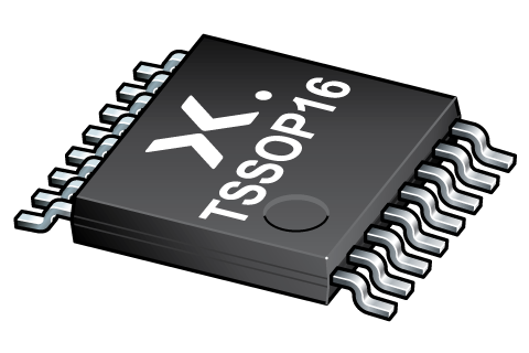
| 74AXP4T245PW | Production | 0.9 - 5.5 | 0.9 - 5.5 | CMOS | ± 12 | 9 | 4 | ultra low | -40~125 | 123 | 4.0 | 52 | TSSOP16 |
| Model Name | 描述 |
|---|---|
|
|
| 型号 | 可订购的器件编号,(订购码(12NC)) | 状态 | 标示 | 封装 | 外形图 | 回流焊/波峰焊 | 包装 |
|---|---|---|---|---|---|---|---|
| 74AXP4T245PW | 74AXP4T245PWJ (935690703118) |
Active | XP4T245 |
TSSOP16 (SOT403-1) |
SOT403-1 |
SSOP-TSSOP-VSO-WAVE
|
SOT403-1_118 |
| 文件名称 | 标题 | 类型 | 日期 |
|---|---|---|---|
| 74AXP4T245 | 4-bit dual supply translating transceiver; 3-state | Data sheet | 2020-02-06 |
| AN90029 | Pin FMEA for AXPnT family | Application note | 2021-07-13 |
| SOT403-1 | 3D model for products with SOT403-1 package | Design support | 2020-01-22 |
| Nexperia_document_leaflet_Logic_AXP_technology_portfolio_201904 | AXP – Extremely low-power logic technology portfolio | Leaflet | 2019-04-05 |
| Nexperia_package_poster | Nexperia package poster | Leaflet | 2020-05-15 |
| TSSOP16_SOT403-1_mk | plastic, thin shrink small outline package; 16 leads; 0.65 mm pitch; 5 mm x 4.4 mm x 1.1 mm body | Marcom graphics | 2017-01-28 |
| SOT403-1 | plastic, thin shrink small outline package; 16 leads; 5 mm x 4.4 mm x 1.2 mm body | Package information | 2023-11-08 |
| SOT403-1_118 | TSSOP16; Reel pack for SMD, 13"; Q1/T1 product orientation | Packing information | 2020-04-21 |
| 74AXP4T245PW_Nexperia_Product_Reliability | 74AXP4T245PW Nexperia Product Reliability | Quality document | 2023-05-29 |
| SSOP-TSSOP-VSO-WAVE | Footprint for wave soldering | Wave soldering | 2009-10-08 |
如果您需要设计/技术支持,请告知我们并填写 应答表 我们会尽快回复您。
| 文件名称 | 标题 | 类型 | 日期 |
|---|---|---|---|
| SOT403-1 | 3D model for products with SOT403-1 package | Design support | 2020-01-22 |
| Model Name | 描述 |
|---|---|
|
|
| 型号 | Orderable part number | Ordering code (12NC) | 状态 | 包装 | Packing Quantity | 在线购买 |
|---|---|---|---|---|---|---|
| 74AXP4T245PW | 74AXP4T245PWJ | 935690703118 | Active | SOT403-1_118 | 2,500 | 订单产品 |
安世半导体客户可通过我们的销售机构或直接通过在线样品商店订购样品: https://extranet.nexperia.com.
样品订单通常需要2-4天寄送时间。
如果您尚未取得安世半导体的直接采购帐号,我们的全球与区域经销网络可以协助您取得样品。
The interactive datasheets are based on the Nexperia MOSFET precision electrothermal models. With our interactive datasheets you can simply specify your own conditions interactively. Start by changing the values of the conditions. You can do this by using the sliders in the condition fields. By dragging the sliders you will see how the MOSFET will perform at the new conditions set.
4-bit dual supply translating transceiver; 3-state
| SKU | 库存* | MOQ | 单位价格 | 数量 |
|---|