
特性
-
Wide supply voltage range:
-
VCC(A): 1.2 V to 5.5 V
-
VCC(B): 1.2 V to 5.5 V
-
-
High noise immunity
-
Complies with JEDEC standards:
-
JESD8-7 (1.2 V to 1.95 V)
-
JESD8-5 (1.8 V to 2.7 V)
-
JESD8C (2.7 V to 3.6 V)
-
JESD36 (4.5 V to 5.5 V)
-
-
Maximum data rates:
-
420 Mbps (3.3 V to 5.0 V translation)
-
210 Mbps (translate to 3.3 V))
-
140 Mbps (translate to 2.5 V)
-
75 Mbps (translate to 1.8 V)
-
60 Mbps (translate to 1.5 V)
-
-
Suspend mode
-
Latch-up performance exceeds 100 mA per JESD 78 Class II
-
±24 mA output drive (VCC = 3.0 V)
-
Inputs accept voltages up to 5.5 V
-
Low power consumption: 16 μA maximum ICC
-
IOFF circuitry provides partial Power-down mode operation
-
ESD protection:
-
HBM: ANSI/ESDA/JEDEC JS-001 class 3A exceeds 4000 V
-
CDM: ANSI/ESDA/JEDEC JS-002 class C3 exceeds 1000 V
-
-
Multiple package options
-
Specified from -40 °C to +85 °C and -40 °C to +125 °C
参数类型
| Type number | Product status | VCC(A) (V) | VCC(B) (V) | Logic switching levels | Output drive capability (mA) | tpd (ns) | Nr of bits | Power dissipation considerations | Tamb (°C) | Rth(j-a) (K/W) | Ψth(j-top) (K/W) | Rth(j-c) (K/W) | Package name |
|---|---|---|---|---|---|---|---|---|---|---|---|---|---|
| 74LVC2T45DC | Production | 1.2 - 5.5 | 1.2 - 5.5 | CMOS/LVTTL | ± 24 | 2.5 | 2 | low | -40~125 | 198 | 30.6 | 107 | VSSOP8 |
| 74LVC2T45GN | Production | 1.2 - 5.5 | 1.2 - 5.5 | CMOS/LVTTL | ± 24 | 2.5 | 2 | low | -40~125 | 224 | 8.3 | 137 | XSON8 |
| 74LVC2T45GS | Production | 1.2 - 5.5 | 1.2 - 5.5 | CMOS/LVTTL | ± 24 | 2.5 | 2 | low | -40~125 | 261 | 8.5 | 136 | XSON8 |
| 74LVC2T45GT | Production | 1.2 - 5.5 | 1.2 - 5.5 | CMOS/LVTTL | ± 24 | 2.5 | 2 | low | -40~125 | 307 | 5.1 | 144 | XSON8 |
| 74LVCH2T45DC | Production | 1.2 - 5.5 | 1.2 - 5.5 | CMOS/LVTTL | ± 24 | 2.5 | 2 | low | -40~125 | 198 | 30.6 | 107 | VSSOP8 |
| 74LVCH2T45GN | Production | 1.2 - 5.5 | 1.2 - 5.5 | CMOS/LVTTL | ± 24 | 2.5 | 2 | low | -40~125 | 224 | 8.3 | 137 | XSON8 |
| 74LVCH2T45GS | Production | 1.2 - 5.5 | 1.2 - 5.5 | CMOS/LVTTL | ± 24 | 2.5 | 2 | low | -40~125 | 261 | 8.5 | 136 | XSON8 |
| 74LVCH2T45GT | Production | 1.2 - 5.5 | 1.2 - 5.5 | CMOS/LVTTL | ± 24 | 2.5 | 2 | low | -40~125 | 307 | 5.1 | 144 | XSON8 |
封装
| 型号 | 封装 | 尺寸版本 | 回流焊/波峰焊 | 包装 | 状态 | 标示 | 可订购的器件编号,(订购码(12NC)) |
|---|---|---|---|---|---|---|---|
| 74LVC2T45DC | 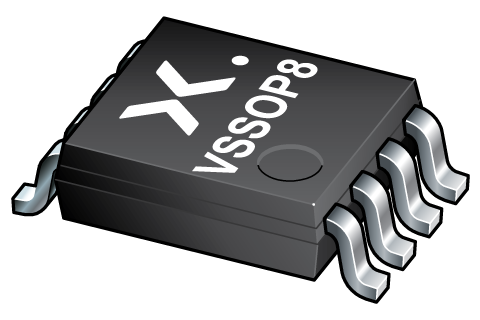 VSSOP8 (SOT765-1) | SOT765-1 | SOT765-1_125 | Active | V45 | 74LVC2T45DC,125 ( 9352 847 57125 ) | |
| 74LVC2T45GN | 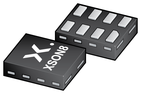 XSON8 (SOT1116) | SOT1116 | REFLOW_BG-BD-1 | SOT1116_115 | Active | V5 | 74LVC2T45GN,115 ( 9352 922 51115 ) |
| 74LVC2T45GS | 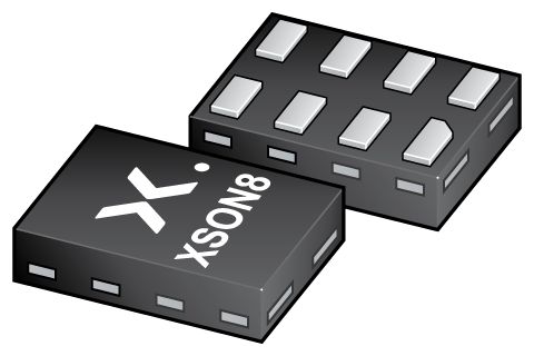 XSON8 (SOT1203) | SOT1203 | REFLOW_BG-BD-1 | SOT1203_115 | Active | V5 | 74LVC2T45GS,115 ( 9352 928 04115 ) |
| 74LVC2T45GT | 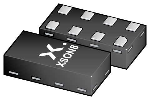 XSON8 (SOT833-1) | SOT833-1 | SOT833-1_115 | Active | V45 | 74LVC2T45GT,115 ( 9352 847 58115 ) | |
| 74LVCH2T45DC | VSSOP8 (SOT765-1) | SOT765-1 | SOT765-1_125 | Active | X45 | 74LVCH2T45DC,125 ( 9352 847 61125 ) | |
| 74LVCH2T45GN | XSON8 (SOT1116) | SOT1116 | REFLOW_BG-BD-1 | SOT1116_115 | Active | X5 | 74LVCH2T45GN,115 ( 9352 922 59115 ) |
| 74LVCH2T45GS | XSON8 (SOT1203) | SOT1203 | REFLOW_BG-BD-1 | SOT1203_115 | Active | X5 | 74LVCH2T45GS,115 ( 9352 928 16115 ) |
| 74LVCH2T45GT | XSON8 (SOT833-1) | SOT833-1 | SOT833-1_115 | Active | X45 | 74LVCH2T45GT,115 ( 9352 847 62115 ) |
环境信息
| 型号 | 可订购的器件编号 | 化学成分 | RoHS | RHF指示符 | 无铅转换日期 |
|---|---|---|---|---|---|
| 74LVC2T45DC | 74LVC2T45DC,125 | 74LVC2T45DC | Always Pb-free | ||
| 74LVC2T45GN | 74LVC2T45GN,115 | 74LVC2T45GN | Always Pb-free | ||
| 74LVC2T45GS | 74LVC2T45GS,115 | 74LVC2T45GS | Always Pb-free | ||
| 74LVC2T45GT | 74LVC2T45GT,115 | 74LVC2T45GT | Always Pb-free | ||
| 74LVCH2T45DC | 74LVCH2T45DC,125 | 74LVCH2T45DC | Always Pb-free | ||
| 74LVCH2T45GN | 74LVCH2T45GN,115 | 74LVCH2T45GN | Always Pb-free | ||
| 74LVCH2T45GS | 74LVCH2T45GS,115 | 74LVCH2T45GS | Always Pb-free | ||
| 74LVCH2T45GT | 74LVCH2T45GT,115 | 74LVCH2T45GT | Always Pb-free |
文档 (15)
| 文件名称 | 标题 | 类型 | 日期 |
|---|---|---|---|
| 74LVC_LVCH2T45 | Dual supply translating transceiver; 3-state | Data sheet | 2023-08-09 |
| AN10161 | PicoGate Logic footprints | Application note | 2002-10-29 |
| AN11009 | Pin FMEA for LVC family | Application note | 2019-01-09 |
| Nexperia_document_guide_Logic_translators | Nexperia Logic Translators | Brochure | 2021-04-12 |
| lvch2t45 | lvch2t45 IBIS model | IBIS model | 2013-04-07 |
| lvc2t45 | lvc2t45 IBIS model | IBIS model | 2013-04-07 |
| MAR_SOT1203 | MAR_SOT1203 Topmark | Top marking | 2013-06-03 |
| SOT1203 | plastic, leadless extremely thin small outline package; 8 terminals; 0.35 mm pitch; 1.35 mm x 1 mm x 0.35 mm body | Package information | 2022-06-03 |
| REFLOW_BG-BD-1 | Reflow soldering profile | Reflow soldering | 2021-04-06 |
| MAR_SOT833 | MAR_SOT833 Topmark | Top marking | 2013-06-03 |
| SOT833-1 | plastic, leadless extremely thin small outline package; 8 terminals; 0.5 mm pitch; 1 mm x 1.95 mm x 0.5 mm body | Package information | 2022-06-03 |
| SOT765-1 | plastic, very thin shrink small outline package; 8 leads; 0.5 mm pitch; 2 mm x 2.3 mm x 1 mm body | Package information | 2022-06-03 |
| MAR_SOT1116 | MAR_SOT1116 Topmark | Top marking | 2013-06-03 |
| SOT1116 | plastic, leadless extremely thin small outline package; 8 terminals; 0.3 mm pitch; 1.2 mm x 1 mm x 0.35 mm body | Package information | 2022-06-02 |
| REFLOW_BG-BD-1 | Reflow soldering profile | Reflow soldering | 2021-04-06 |
支持
如果您需要设计/技术支持,请告知我们并填写 应答表, 我们会尽快回复您。
样品
安世半导体客户可通过我们的销售机构或直接通过在线样品商店订购样品: https://extranet.nexperia.com.
样品订单通常需要2-4天寄送时间。
如果您尚未取得安世半导体的直接采购帐号,我们的全球与区域经销网络可以协助您取得样品。