Register once, drag and drop ECAD models into your CAD tool and speed up your design.
Click here for more information74AVC1T1004GU33
1-to-4 fan-out buffer
The 74AVC1T1004 is a translating 1-to-4 fan-out buffer suitable for use in clock distribution. It has dual supplies (VCC(A) and VCC(B)) for voltage translation. It also has a data input (A), four data outputs (Yn) and an output enable input (OE). VCC(A) and VCC(B) can be independently supplied at any voltage between 0.8 V and 3.6 V. It makes the device suitable for low voltage translation between any of the following voltages: 0.8 V, 1.2 V, 1.5 V, 1.8 V, 2.5 V and 3.3 V. The levels of A and OE are referenced to VCC(A), outputs Yn are referenced to VCC(B). This supply configuration ensures that the fanned out signals can be used in level shifting. A HIGH on OE causes all outputs to be pulled LOW via pull-down resistors, a LOW on OE disconnects the pull-down resistors and enables all outputs.
Schmitt trigger action at all inputs makes the circuit tolerant for slower input rise and fall time.
The IOFF circuitry disables the output, preventing any damaging backflow current through the device when it is powered down.
Features and benefits
Wide supply voltage range:
VCC(A): 0.8 V to 3.6 V
VCC(B): 0.8 V to 3.6 V
Complies with JEDEC standards:
JESD8-12 (0.8 V to 1.3 V)
JESD8-11 (0.9 V to 1.65 V)
JESD8-7 (1.2 V to 1.95 V)
JESD8-5 (1.8 V to 2.7 V)
JESD8-B (2.7 V to 3.6 V)
ESD protection:
HBM ANSI/ESDA/JEDEC JS-001 Class 2 exceeds 2 kV
CDM JESD22-C101 exceeds 1 kV
Maximum data rates:
380 Mbit/s (≥ 1.8 V to 3.3 V translation)
200 Mbit/s (≥ 1.1 V to 3.3 V translation)
200 Mbit/s (≥ 1.1 V to 2.5 V translation)
200 Mbit/s (≥ 1.1 V to 1.8 V translation)
150 Mbit/s (≥ 1.1 V to 1.5 V translation)
100 Mbit/s (≥ 1.1 V to 1.2 V translation)
Latch-up performance exceeds 100 mA per JESD 78 Class II
Inputs accept voltages up to 3.6 V
Specified from -40 °C to +85 °C and -40 °C to +125 °C
参数类型
| 型号 | Product status | VCC(A) (V) | VCC(B) (V) | Logic switching levels | Output drive capability (mA) | tpd (ns) | Nr of bits | Power dissipation considerations | Package name |
|---|---|---|---|---|---|---|---|---|---|
| 74AVC1T1004GU33 | End of life | 0.8 - 3.6 | 0.8 - 3.6 | CMOS/LVTTL | ± 12 | 4.9 | 1 | very low | X2QFN10 |
封装
下表中的所有产品型号均已停产 。
| 型号 | 可订购的器件编号,(订购码(12NC)) | 状态 | 标示 | 封装 | 外形图 | 回流焊/波峰焊 | 包装 |
|---|---|---|---|---|---|---|---|
| 74AVC1T1004GU33 | 74AVC1T1004GU33Z (935690126471) |
Withdrawn / End-of-life | Bc |
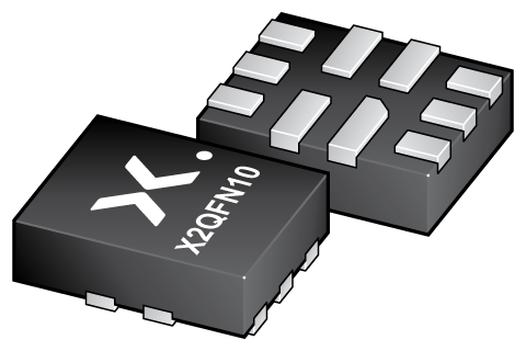
X2QFN10 (SOT1430-1) |
SOT1430-1 | SOT1430-1_471 |
环境信息
下表中的所有产品型号均已停产 。
| 型号 | 可订购的器件编号 | 化学成分 | RoHS | RHF指示符 |
|---|---|---|---|---|
| 74AVC1T1004GU33 | 74AVC1T1004GU33Z | 74AVC1T1004GU33 |
|
|
Series
文档 (4)
| 文件名称 | 标题 | 类型 | 日期 |
|---|---|---|---|
| AN90007 | Pin FMEA for AVC family | Application note | 2018-11-30 |
| avc1t1004 | 74AVC1T1004 IBIS model | IBIS model | 2018-06-18 |
| Nexperia_package_poster | Nexperia package poster | Leaflet | 2020-05-15 |
| SOT1430-1 | plastic, leadless extremely thin small outline package; 10 terminals; body 1.6 x 1.3 x 0.33 mm | Package information | 2020-04-21 |
支持
如果您需要设计/技术支持,请告知我们并填写 应答表 我们会尽快回复您。
模型
| 文件名称 | 标题 | 类型 | 日期 |
|---|---|---|---|
| avc1t1004 | 74AVC1T1004 IBIS model | IBIS model | 2018-06-18 |
How does it work?
The interactive datasheets are based on the Nexperia MOSFET precision electrothermal models. With our interactive datasheets you can simply specify your own conditions interactively. Start by changing the values of the conditions. You can do this by using the sliders in the condition fields. By dragging the sliders you will see how the MOSFET will perform at the new conditions set.
74AVC1T1004GU33
1-to-4 fan-out buffer
从安世半导体购买
| SKU | 库存* | MOQ | 单位价格 | 数量 |
|---|