
Register once, drag and drop ECAD models into your CAD tool and speed up your design.
Click here for more information74LV00DB
Quad 2-input NAND gate
74LV00是低压硅栅CMOS器件,与74HC00和74HCT00针脚和功能兼容。
74LV00提供四路2输入与非功能。
该产品已停产。参见单击此处了解停产信息和替代产品。
Alternatives
Features and benefits
- 宽工作电压范围:1.0 V至5.5 V
- 最适合低压应用:1.0 V至3.6 V
- 接受介于VCC = 2.7 V和VCC = 3.6 V之间的TTL输入电平
- VCC = 3.3 V且Tamb = 25 °C时的典型输出地弹:< 0.8 V
- VCC = 3.3 V且Tamb = 25 °C时的典型高电平输出电压(VOH)欠冲:> 2 V
- ESD保护:
- HBM JESD22-A114E超过2000 V
- MM JESD22-A115-A超过200 V
- 多种封装选择
- 额定温度范围为-40 °C至+85 °C和-40 °C至+125 °C
参数类型
| 型号 | Product status | Package name |
|---|---|---|
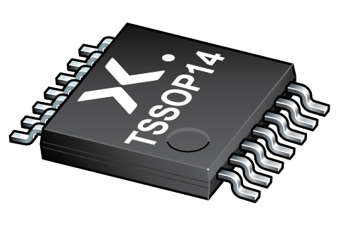
| 74LV00DB | End of life | SSOP14 |
PCB Symbol, Footprint and 3D Model
| Model Name | 描述 |
|---|---|
|
|
封装
下表中的所有产品型号已停产。参见表 停产信息 了解更多信息。
| 型号 | 可订购的器件编号,(订购码(12NC)) | 状态 | 标示 | 封装 | 外形图 | 回流焊/波峰焊 | 包装 |
|---|---|---|---|---|---|---|---|
| 74LV00DB | 74LV00DB,112 (935170130112) |
Obsolete | no package information | ||||
| 74LV00DB,118 (935170130118) |
Obsolete | ||||||
环境信息
下表中的所有产品型号已停产。参见表 停产信息 了解更多信息。
| 型号 | 可订购的器件编号 | 化学成分 | RoHS | RHF指示符 |
|---|---|---|---|---|
| 74LV00DB | 74LV00DB,112 | 74LV00DB |
|
|
| 74LV00DB | 74LV00DB,118 | 74LV00DB |
|
|
How does it work?
The interactive datasheets are based on the Nexperia MOSFET precision electrothermal models. With our interactive datasheets you can simply specify your own conditions interactively. Start by changing the values of the conditions. You can do this by using the sliders in the condition fields. By dragging the sliders you will see how the MOSFET will perform at the new conditions set.
74LV00DB
Quad 2-input NAND gate
从安世半导体购买
| SKU | 库存* | MOQ | 单位价格 | 数量 |
|---|