
Register once, drag and drop ECAD models into your CAD tool and speed up your design.
Click here for more informationHEF4002BT
Dual 4-input NOR gate
The HEF4002B is a dual 4-input NOR gate. The outputs are fully buffered for highest noise immunity and pattern insensitivity to output impedance variations..
It operates over a recommended VDD power supply range of 3 V to 15 V referenced to VSS (usually ground). Unused inputs must be connected to VDD, VSS, or another input.
Features and benefits
Fully static operation
5 V, 10 V, and 15 V parametric ratings
Standardized symmetrical output characteristics
Inputs and outputs are protected against electrostatic effects
Specified from —40 °C to +85 °C
Complies with JEDEC standard JESD 13-B
参数类型
| 型号 | Product status | VCC (V) | Logic switching levels | Output drive capability (mA) | tpd (ns) | fmax (MHz) | Nr of bits | Power dissipation considerations | Tamb (°C) | Rth(j-a) (K/W) | Ψth(j-top) (K/W) | Rth(j-c) (K/W) | Package name |
|---|---|---|---|---|---|---|---|---|---|---|---|---|---|
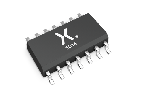
| HEF4002BT | End of life | 3.0 - 15 | CMOS | ± 2.4 | 20 | 10 | 4 | medium | -40~85 | 89 | 7.5 | 47 | SO14 |
PCB Symbol, Footprint and 3D Model
| Model Name | 描述 |
|---|---|
|
|
封装
下表中的所有产品型号均已停产 。
| 型号 | 可订购的器件编号,(订购码(12NC)) | 状态 | 标示 | 封装 | 外形图 | 回流焊/波峰焊 | 包装 |
|---|---|---|---|---|---|---|---|
| HEF4002BT | HEF4002BT,652 (933372600652) |
Withdrawn / End-of-life | HEF4002BT |
SO14 (SOT108-1) |
SOT108-1 |
SO-SOJ-REFLOW
SO-SOJ-WAVE WAVE_BG-BD-1 |
SOT108-1_652 |
| HEF4002BT,653 (933372600653) |
Obsolete | HEF4002BT | Not available |
环境信息
下表中的所有产品型号均已停产 。
| 型号 | 可订购的器件编号 | 化学成分 | RoHS | RHF指示符 |
|---|---|---|---|---|
| HEF4002BT | HEF4002BT,652 | HEF4002BT |
|
|
| HEF4002BT | HEF4002BT,653 | HEF4002BT |
|
|
文档 (10)
| 文件名称 | 标题 | 类型 | 日期 |
|---|---|---|---|
| HEF4002B | Dual 4-input NOR gate | Data sheet | 2017-03-17 |
| AN11051 | Pin FMEA HEF4000 family | Application note | 2019-01-09 |
| SOT108-1 | 3D model for products with SOT108-1 package | Design support | 2020-01-22 |
| Nexperia_package_poster | Nexperia package poster | Leaflet | 2020-05-15 |
| SO14_SOT108-1_mk | plastic, small outline package; 14 leads; 1.27 mm pitch; 8.65 mm x 3.9 mm x 1.75 mm body | Marcom graphics | 2017-01-28 |
| familyhef4000specification | HEF/HEC4000B family specification overview | Other type | 2012-05-23 |
| SOT108-1 | plastic, small outline package; 14 leads; 1.27 mm pitch; 8.65 mm x 3.9 mm x 1.75 mm body | Package information | 2023-11-07 |
| SO-SOJ-REFLOW | Footprint for reflow soldering | Reflow soldering | 2009-10-08 |
| SO-SOJ-WAVE | Footprint for wave soldering | Wave soldering | 2009-10-08 |
| WAVE_BG-BD-1 | Wave soldering profile | Wave soldering | 2021-09-08 |
支持
如果您需要设计/技术支持,请告知我们并填写 应答表 我们会尽快回复您。
模型
| 文件名称 | 标题 | 类型 | 日期 |
|---|---|---|---|
| SOT108-1 | 3D model for products with SOT108-1 package | Design support | 2020-01-22 |
PCB Symbol, Footprint and 3D Model
| Model Name | 描述 |
|---|---|
|
|
How does it work?
The interactive datasheets are based on the Nexperia MOSFET precision electrothermal models. With our interactive datasheets you can simply specify your own conditions interactively. Start by changing the values of the conditions. You can do this by using the sliders in the condition fields. By dragging the sliders you will see how the MOSFET will perform at the new conditions set.
HEF4002BT
Dual 4-input NOR gate
从安世半导体购买
| SKU | 库存* | MOQ | 单位价格 | 数量 |
|---|