Register once, drag and drop ECAD models into your CAD tool and speed up your design.
Click here for more information74LVC16374ADL
16-bit edge-triggered D-type flip-flop; 5 V tolerant; 3-state
74LVC16374A和74LVCH16374A是16位边沿触发式触发器,具有用于每个触发器总线保持(仅74LVCH16374A)的独立D类输入以及用于总线应用的三态输出。它由八个正沿触发式触发器的两部分组成。每个八路器件都具有一个时钟输入(nCP)和一个输出使能(nOE)。
触发器会存储它们各自的D输入状态,满足时钟(CP)从低到高转换的建立和保持时间要求。
引脚nOE为低电平时,触发器的内容在输出处可用。引脚nOE为高电平时,输出会进入高阻抗关断状态。输入nOE的操作不会影响触发器的状态。
输入可从3.3 V器件或5 V器件驱动。禁用时,输出上最多可施加5.5 V的电压。这些特性允许在3.3 V和5 V混合电压应用中使用这些器件。
总线保持数据输入无需用外部上拉电阻来保持闲置输入。
Alternatives
Features and benefits
- 与5 V逻辑器件连接的5 V容压输入/输出
- 1.2 V至3.6 V的宽电源电压范围
- CMOS低功耗
- MULTIBYTE直通标准引脚排列架构
- 用于最大程度减少噪声和接地反弹的多个低电感电源引脚
- 直接与TTL电平连接
- 所有数据输入具有总线保持(仅针对74LVCH16374A)
- 高阻抗输出(VCC = 0 V时)
- 符合JEDEC标准:
- JESD8-7A(1.65 V至1.95 V)
- JESD8-5A(2.3 V至2.7 V)
- JESD8-C/JESD36(2.7 V至3.6 V)
- ESD保护:
- HBM JESD22-A114F超过2000 V
- MM JESD22-A115-B超过200 V
- CDM JESD22-C101E超过1000 V
- 指定温度范围为-40 °C至+85 °C和-40 °C至+125 °C
参数类型
| 型号 | Product status | Package name |
|---|---|---|
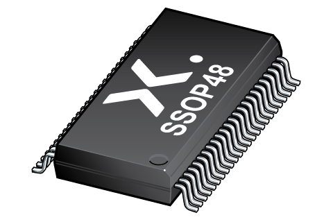
| 74LVC16374ADL | End of life | SSOP48 |
PCB Symbol, Footprint and 3D Model
| Model Name | 描述 |
|---|---|
|
|
封装
下表中的所有产品型号已停产。参见表 停产信息 了解更多信息。
| 型号 | 可订购的器件编号,(订购码(12NC)) | 状态 | 标示 | 封装 | 外形图 | 回流焊/波峰焊 | 包装 |
|---|---|---|---|---|---|---|---|
| 74LVC16374ADL | 74LVC16374ADL,112 (935235180112) |
Withdrawn / End-of-life | LVC16374A |
SSOP48 (SOT370-1) |
SOT370-1 |
SSOP-TSSOP-VSO-REFLOW
SSOP-TSSOP-VSO-WAVE |
Not available |
| 74LVC16374ADL,118 (935235180118) |
Withdrawn / End-of-life | LVC16374A | SOT370-1_118 |
环境信息
下表中的所有产品型号已停产。参见表 停产信息 了解更多信息。
| 型号 | 可订购的器件编号 | 化学成分 | RoHS | RHF指示符 |
|---|---|---|---|---|
| 74LVC16374ADL | 74LVC16374ADL,112 | 74LVC16374ADL |
|
|
| 74LVC16374ADL | 74LVC16374ADL,118 | 74LVC16374ADL |
|
|
Series
文档 (8)
| 文件名称 | 标题 | 类型 | 日期 |
|---|---|---|---|
| 74LVC_LVCH16374A | 16-bit edge-triggered D-type flip-flop; 5 V tolerant; 3-state | Data sheet | 2023-08-01 |
| AN11009 | Pin FMEA for LVC family | Application note | 2019-01-09 |
| AN263 | Power considerations when using CMOS and BiCMOS logic devices | Application note | 2023-02-07 |
| lvc16374a | lvc16374a IBIS model | IBIS model | 2013-04-07 |
| Nexperia_package_poster | Nexperia package poster | Leaflet | 2020-05-15 |
| SOT370-1 | plastic, shrink small outline package; 48 leads; 0.635 mm pitch; 15.9 mm x 7.5 mm x 2.8 mm body | Package information | 2020-04-21 |
| SSOP-TSSOP-VSO-REFLOW | Footprint for reflow soldering | Reflow soldering | 2009-10-08 |
| SSOP-TSSOP-VSO-WAVE | Footprint for wave soldering | Wave soldering | 2009-10-08 |
支持
如果您需要设计/技术支持,请告知我们并填写 应答表 我们会尽快回复您。
模型
| 文件名称 | 标题 | 类型 | 日期 |
|---|---|---|---|
| lvc16374a | lvc16374a IBIS model | IBIS model | 2013-04-07 |
PCB Symbol, Footprint and 3D Model
| Model Name | 描述 |
|---|---|
|
|
How does it work?
The interactive datasheets are based on the Nexperia MOSFET precision electrothermal models. With our interactive datasheets you can simply specify your own conditions interactively. Start by changing the values of the conditions. You can do this by using the sliders in the condition fields. By dragging the sliders you will see how the MOSFET will perform at the new conditions set.
74LVC16374ADL
16-bit edge-triggered D-type flip-flop; 5 V tolerant; 3-state
从安世半导体购买
| SKU | 库存* | MOQ | 单位价格 | 数量 |
|---|