Register once, drag and drop ECAD models into your CAD tool and speed up your design.
Click here for more information74LVC162373ADL
16-bit D-type transparent latch; 30 Ohm series termination resistors; 5 V tolerant inputs/outputs; 3-state
The 74LVC162373A and 74LVCH162373A are 16-bit D-type transparent latches with 30 Ω termination resistors and 3-state outputs. The 74LVCH162373A has separate D-type inputs with bus hold for each latch. Both devices can be used as two 8-bit transparent latches or a single 16-bit transparent latch. Both devices feature two latch enables (1LE and 2LE) and two output enables (1OE and 2OE), each controlling 8-bits. When nLE is HIGH, data at the inputs enter the latches. In this condition the latches are transparent, a latch output will change each time its corresponding D-input changes. When nLE is LOW the latches store the information that was present at the inputs a set-up time preceding the HIGH-to-LOW transition of nLE. A HIGH on nOE causes the outputs to assume a high-impedance OFF-state. Operation of the nOE input does not affect the state of the latches. Inputs can be driven from either 3.3 V or 5 V devices. This feature allows the use of these devices as translators in mixed 3.3 V and 5 V environments.
Schmitt-trigger action at all inputs makes the circuit tolerant of slower input rise and fall times.
These devices are fully specified for partial power down applications using IOFF. The IOFF circuitry disables the output, preventing the potentially damaging backflow current through the devices when they are powered down.
Alternatives
Features and benefits
Overvoltage tolerant inputs to 5.5 V
Wide supply voltage range from 1.2 V to 3.6 V
CMOS low power consumption
Multibyte flow-through standard pinout architecture
Multiple low inductance supply pins for minimum noise and ground bounce
Direct interface with TTL levels
All data inputs have bus hold (74LVCH162373A only)
IOFF circuitry provides partial Power-down mode operation
Complies with JEDEC standard:
- JESD8-7A (1.65 V to 1.95 V)
- JESD8-5A (2.3 V to 2.7 V)
- JESD8-C/JESD36 (2.7 V to 3.6 V)
ESD protection:
HBM: ANSI/ESDA/JEDEC JS-001 class 2 exceeds 2000 V
CDM: ANSI/ESDA/JEDEC JS-002 class C3 exceeds 1000 V
Specified from -40 °C to +85 °C and -40 °C to +125 °C
参数类型
| 型号 | Product status | Package name |
|---|---|---|
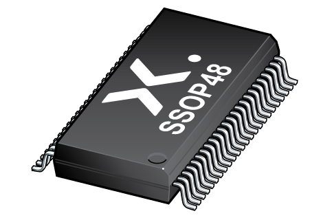
| 74LVC162373ADL | End of life | SSOP48 |
PCB Symbol, Footprint and 3D Model
| Model Name | 描述 |
|---|---|
|
|
封装
下表中的所有产品型号均已停产 。
| 型号 | 可订购的器件编号,(订购码(12NC)) | 状态 | 标示 | 封装 | 外形图 | 回流焊/波峰焊 | 包装 |
|---|---|---|---|---|---|---|---|
| 74LVC162373ADL | 74LVC162373ADL,112 (935237710112) |
Obsolete | LVC162373A |
SSOP48 (SOT370-1) |
SOT370-1 |
SSOP-TSSOP-VSO-REFLOW
SSOP-TSSOP-VSO-WAVE |
Not available |
| 74LVC162373ADL,118 (935237710118) |
Obsolete | LVC162373A | SOT370-1_118 |
环境信息
下表中的所有产品型号均已停产 。
| 型号 | 可订购的器件编号 | 化学成分 | RoHS | RHF指示符 |
|---|---|---|---|---|
| 74LVC162373ADL | 74LVC162373ADL,112 | 74LVC162373ADL |
|
|
| 74LVC162373ADL | 74LVC162373ADL,118 | 74LVC162373ADL |
|
|
Series
文档 (8)
| 文件名称 | 标题 | 类型 | 日期 |
|---|---|---|---|
| 74LVC_LVCH162373A | 16-bit D-type transparent latch; 30 Ohm series termination resistors; 5 V tolerant inputs/outputs; 3-state | Data sheet | 2024-04-03 |
| AN11009 | Pin FMEA for LVC family | Application note | 2019-01-09 |
| AN263 | Power considerations when using CMOS and BiCMOS logic devices | Application note | 2023-02-07 |
| lvc162373a | lvc162373a IBIS model | IBIS model | 2013-04-07 |
| Nexperia_package_poster | Nexperia package poster | Leaflet | 2020-05-15 |
| SOT370-1 | plastic, shrink small outline package; 48 leads; 0.635 mm pitch; 15.9 mm x 7.5 mm x 2.8 mm body | Package information | 2020-04-21 |
| SSOP-TSSOP-VSO-REFLOW | Footprint for reflow soldering | Reflow soldering | 2009-10-08 |
| SSOP-TSSOP-VSO-WAVE | Footprint for wave soldering | Wave soldering | 2009-10-08 |
支持
如果您需要设计/技术支持,请告知我们并填写 应答表 我们会尽快回复您。
模型
| 文件名称 | 标题 | 类型 | 日期 |
|---|---|---|---|
| lvc162373a | lvc162373a IBIS model | IBIS model | 2013-04-07 |
PCB Symbol, Footprint and 3D Model
| Model Name | 描述 |
|---|---|
|
|
How does it work?
The interactive datasheets are based on the Nexperia MOSFET precision electrothermal models. With our interactive datasheets you can simply specify your own conditions interactively. Start by changing the values of the conditions. You can do this by using the sliders in the condition fields. By dragging the sliders you will see how the MOSFET will perform at the new conditions set.
74LVC162373ADL
16-bit D-type transparent latch; 30 Ohm series termination resistors; 5 V tolerant inputs/outputs; 3-state
从安世半导体购买
| SKU | 库存* | MOQ | 单位价格 | 数量 |
|---|