
特性
-
Wide supply voltage range from 0.8 V to 3.6 V
-
High noise immunity
-
CMOS low power dissipation
-
Low static power consumption; ICC = 0.9 μA (maximum)
-
Latch-up performance exceeds 100 mA per JESD78B Class II
-
Overvoltage tolerant inputs to 3.6 V
-
Low noise overshoot and undershoot < 10 % of VCC
-
Input-disable feature allows floating input conditions
-
IOFF circuitry provides partial Power-down mode operation
-
Latch-up performance exceeds 100 mA per JESD 78 Class II Level B
-
Complies with JEDEC standards:
-
JESD8-12 (0.8 V to 1.3 V)
-
JESD8-11 (0.9 V to 1.65 V)
-
JESD8-7 (1.2 V to 1.95 V)
-
JESD8-5 (1.8 V to 2.7 V)
-
JESD8-B (2.7 V to 3.6 V)
-
-
ESD protection:
-
HBM: ANSI/ESDA/JEDEC JS-001 class 3A exceeds 5000 V
-
CDM: ANSI/ESDA/JEDEC JS-002 class C3 exceeds 1000 V
-
-
Multiple package options
-
Specified from -40 °C to +85 °C and -40 °C to +125 °C
参数类型
| Type number | Product status | VCC (V) | Logic switching levels | Output drive capability (mA) | fmax (MHz) | Nr of bits | Power dissipation considerations | Tamb (°C) | Rth(j-a) (K/W) | Rth(j-c) (K/W) | Package name |
|---|---|---|---|---|---|---|---|---|---|---|---|
| 74AUP2G125DC | Production | 0.8 - 3.6 | CMOS | ± 1.9 | 70 | 2 | ultra low | -40~125 | 203 | 113 | VSSOP8 |
| 74AUP2G125GN | Production | 0.8 - 3.6 | CMOS | ± 1.9 | 70 | 2 | ultra low | -40~125 | 238 | 148 | XSON8 |
| 74AUP2G125GS | Production | 0.8 - 3.6 | CMOS | ± 1.9 | 70 | 2 | ultra low | -40~125 | 276 | 146 | XSON8 |
| 74AUP2G125GT | Production | 0.8 - 3.6 | CMOS | ± 1.9 | 70 | 2 | ultra low | -40~125 | 327 | 157 | XSON8 |
| 74AUP2G125GX | Production | 0.8 - 3.6 | CMOS | ± 1.9 | 70 | 2 | ultra low | -40~125 | - | - | X2SON8 |
封装
| 型号 | 封装 | 尺寸版本 | 回流焊/波峰焊 | 包装 | 状态 | 标示 | 可订购的器件编号,(订购码(12NC)) |
|---|---|---|---|---|---|---|---|
| 74AUP2G125DC | 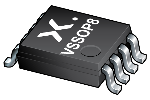 VSSOP8 (SOT765-1) | SOT765-1 | SOT765-1_125 | Active | p25 | 74AUP2G125DC,125 ( 9352 807 27125 ) | |
| 74AUP2G125GN | 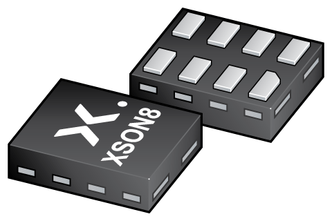 XSON8 (SOT1116) | SOT1116 | REFLOW_BG-BD-1 | SOT1116_115 | Active | aM | 74AUP2G125GN,115 ( 9352 889 88115 ) |
| 74AUP2G125GS | 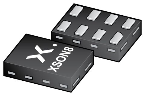 XSON8 (SOT1203) | SOT1203 | REFLOW_BG-BD-1 | SOT1203_115 | Active | aM | 74AUP2G125GS,115 ( 9352 927 82115 ) |
| 74AUP2G125GT | 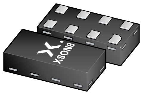 XSON8 (SOT833-1) | SOT833-1 | SOT833-1_115 | Active | p25 | 74AUP2G125GT,115 ( 9352 807 28115 ) | |
| 74AUP2G125GX | 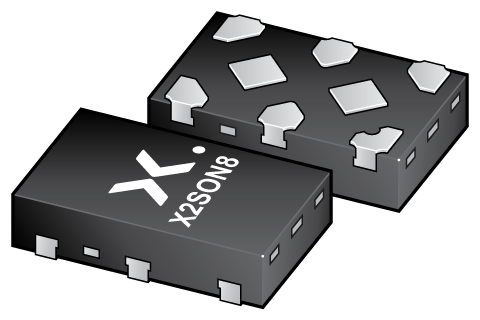 X2SON8 (SOT1233-2) | SOT1233-2 | SOT1233-2_115 | Active | aM | 74AUP2G125GXX ( 9353 084 42115 ) |
环境信息
| 型号 | 可订购的器件编号 | 化学成分 | RoHS | RHF指示符 | 无铅转换日期 |
|---|---|---|---|---|---|
| 74AUP2G125DC | 74AUP2G125DC,125 | 74AUP2G125DC | Always Pb-free | ||
| 74AUP2G125GN | 74AUP2G125GN,115 | 74AUP2G125GN | Always Pb-free | ||
| 74AUP2G125GS | 74AUP2G125GS,115 | 74AUP2G125GS | Always Pb-free | ||
| 74AUP2G125GT | 74AUP2G125GT,115 | 74AUP2G125GT | Always Pb-free | ||
| 74AUP2G125GX | 74AUP2G125GXX | 74AUP2G125GX | week 25, 2019 |
文档 (17)
| 文件名称 | 标题 | 类型 | 日期 |
|---|---|---|---|
| 74AUP2G125 | Low-power dual buffer/line driver; 3-state | Data sheet | 2023-07-26 |
| AN10161 | PicoGate Logic footprints | Application note | 2002-10-29 |
| AN11052 | Pin FMEA for AUP family | Application note | 2019-01-09 |
| aup2g125 | aup2g125 IBIS model | IBIS model | 2013-04-07 |
| Nexperia_document_leaflet_Logic_X2SON_packages_062018 | X2SON ultra-small 4, 5, 6 & 8-pin leadless packages | Leaflet | 2018-06-05 |
| Nexperia_document_leaflet_Logic_AUP_technology_portfolio_201904 | Nexperia_document_leaflet_Logic_AUP_technology_portfolio_201904 | Leaflet | 2019-04-12 |
| Nexperia_Selection_guide_2023 | Nexperia Selection Guide 2023 | Selection guide | 2023-05-10 |
| SOT1233-2 | plastic thermal enhanced extremely thin small outline package; no leads;8 terminals; body 1.35 x 0.8 x 0.32 mm | Package information | 2022-04-21 |
| MAR_SOT1203 | MAR_SOT1203 Topmark | Top marking | 2013-06-03 |
| SOT1203 | plastic, leadless extremely thin small outline package; 8 terminals; 0.35 mm pitch; 1.35 mm x 1 mm x 0.35 mm body | Package information | 2022-06-03 |
| REFLOW_BG-BD-1 | Reflow soldering profile | Reflow soldering | 2021-04-06 |
| MAR_SOT833 | MAR_SOT833 Topmark | Top marking | 2013-06-03 |
| SOT833-1 | plastic, leadless extremely thin small outline package; 8 terminals; 0.5 mm pitch; 1 mm x 1.95 mm x 0.5 mm body | Package information | 2022-06-03 |
| SOT765-1 | plastic, very thin shrink small outline package; 8 leads; 0.5 mm pitch; 2 mm x 2.3 mm x 1 mm body | Package information | 2022-06-03 |
| MAR_SOT1116 | MAR_SOT1116 Topmark | Top marking | 2013-06-03 |
| SOT1116 | plastic, leadless extremely thin small outline package; 8 terminals; 0.3 mm pitch; 1.2 mm x 1 mm x 0.35 mm body | Package information | 2022-06-02 |
| REFLOW_BG-BD-1 | Reflow soldering profile | Reflow soldering | 2021-04-06 |
样品
安世半导体客户可通过我们的销售机构或直接通过在线样品商店订购样品: https://extranet.nexperia.com.
样品订单通常需要2-4天寄送时间。
如果您尚未取得安世半导体的直接采购帐号,我们的全球与区域经销网络可以协助您取得样品。