


74AHC377-Q100; 74AHCT377-Q100
Octal D-type flip-flop with data enable; positive-edge trigger
The 74AHC377-Q100; 74AHCT377-Q100 is a high-speed Si-gate CMOS device and is pin compatible with Low-power Schottky TTL (LSTTL). It is specified in compliance with JEDEC standard No. 7-A. The 74AHC377-Q100; 74AHCT377-Q100 has eight edge-triggered, D-type flip-flops with individual D inputs and Q outputs. A common clock input (CP) loads all flip-flops simultaneously when the data enable input (E) is LOW. The state of each D input, one set-up time before the LOW-to-HIGH clock transition, is transferred to the corresponding output (Qn) of the flip-flop. The E input is only required to be stable one set-up time prior to the LOW-to-HIGH transition for predictable operation.
This product has been qualified to the Automotive Electronics Council (AEC) standard Q100 (Grade 1) and is suitable for use in automotive applications.
Features and benefits
- Automotive product qualification in accordance with AEC-Q100 (Grade 1)
- Specified from ‑40 °C to +85 °C and from ‑40 °C to +125 °C
- Balanced propagation delays
- All inputs have Schmitt-trigger actions
- Inputs accept voltages higher than VCC
- Ideal for addressable register applications
- Data enable for address and data synchronization
- Eight positive-edge triggered D-type flip-flops
- Input levels:
- For 74AHC377-Q100: CMOS level
- For 74AHCT377-Q100: TTL level
- ESD protection:
- MIL-STD-883, method 3015 exceeds 2000 V
- HBM JESD22-A114F exceeds 2000 V
- MM JESD22-A115-A exceeds 200 V (C = 200 pF, R = 0 Ω)
- Multiple package options
Applications
封装
下表中的所有产品型号均已停产 。
| 型号 | 可订购的器件编号,(订购码(12NC)) | 状态 | 标示 | 封装 | 外形图 | 回流焊/波峰焊 | 包装 |
|---|---|---|---|---|---|---|---|
| 74AHC377D-Q100 | 74AHC377D‑Q100J (935303408118) |
Obsolete | no package information | ||||
| 74AHC377PW-Q100 | 74AHC377PW‑Q100J (935301377118) |
Obsolete |
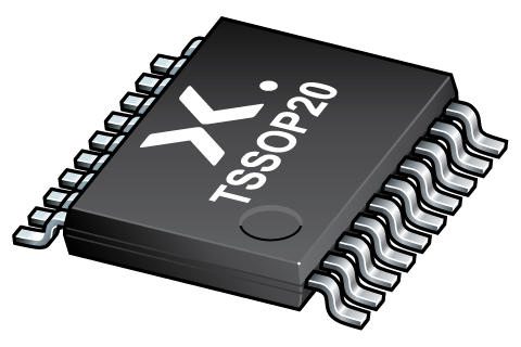
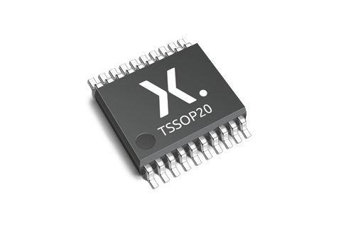
TSSOP20 (SOT360-1) |
SOT360-1 |
SSOP-TSSOP-VSO-WAVE
|
SOT360-1_118 | |
| 74AHCT377D-Q100 | 74AHCT377D‑Q100J (935301388118) |
Obsolete | no package information | ||||
| 74AHCT377PW-Q100 | 74AHCT377PW‑Q100J (935301208118) |
Obsolete | no package information | ||||
环境信息
下表中的所有产品型号均已停产 。
| 型号 | 可订购的器件编号 | 化学成分 | RoHS | RHF指示符 |
|---|---|---|---|---|
| 74AHC377D-Q100 | 74AHC377D‑Q100J | 74AHC377D‑Q100 |
|
|
| 74AHC377PW-Q100 | 74AHC377PW‑Q100J | 74AHC377PW‑Q100 |
|
|
| 74AHCT377D-Q100 | 74AHCT377D‑Q100J | 74AHCT377D‑Q100 |
|
|
| 74AHCT377PW-Q100 | 74AHCT377PW‑Q100J | 74AHCT377PW‑Q100 |
|
|
文档 (9)
| 文件名称 | 标题 | 类型 | 日期 |
|---|---|---|---|
| 74AHC_AHCT377_Q100 | Octal D-type flip-flop with data enable; positive-edge trigger | Data sheet | 2017-05-03 |
| AN90063 | Questions about package outline drawings | Application note | 2025-10-22 |
| SOT360-1 | 3D model for products with SOT360-1 package | Design support | 2020-01-22 |
| ahc377 | ahc377 IBIS model | IBIS model | 2013-04-08 |
| ahct377 | ahct377 IBIS model | IBIS model | 2013-04-08 |
| Nexperia_package_poster | Nexperia package poster | Leaflet | 2020-05-15 |
| TSSOP20_SOT360-1_mk | plastic, thin shrink small outline package; 20 leads; 0.65 mm pitch; 6.5 mm x 4.4 mm x 1.1 mm body | Marcom graphics | 2017-01-28 |
| SOT360-1 | plastic, thin shrink small outline package; 20 leads; 0.65 mm pitch; 6.5 mm x 4.4 mm x 1.2 mm body | Package information | 2024-11-15 |
| SSOP-TSSOP-VSO-WAVE | Footprint for wave soldering | Wave soldering | 2009-10-08 |
支持
如果您需要设计/技术支持,请告知我们并填写 应答表 我们会尽快回复您。
Ordering, pricing & availability
样品
作为 Nexperia 的客户,您可以通过我们的销售机构订购样品。
如果您没有 Nexperia 的直接账户,我们的全球和地区分销商网络可为您提供 Nexperia 样品支持。查看官方经销商列表。