


Author: Christopher Liu, Applications Engineer, Manchester
This interactive application note contains an embedded Cloud based simulation to augment the text.
To open the embedded simulation, simply hover over the simulation image. Left click anywhere in the graphic area once the central play button changes in colour. This opens the schematic in the Cloud environment. See the interactive application note tutorial page for more details on how to use the simulations.
See related application note: AN90013 LFPAK MOSFET thermal design guide
1. Introduction
Power MOSFETs provide efficient conversion and supply of power in a wide variety of automotive, industrial and consumer applications. However, no MOSFET is 100% efficient and as such they exhibit three types of power losses during normal operation:
- Switching losses during the transitional phase, see Fig 1.
- Conduction losses during the on-state, see Fig 1.
- Avalanche losses if breakdown voltage is exceeded when driving an inductive load, see Fig 2.

Figure 1. MOSFET turn-on waveforms

Figure 2. MOSFET turn-off avalanche waveforms
The culmination of these power losses can result in thermal overstress and failure of the MOSFET if not sufficiently accounted for in a PCB design. Therefore, it is necessary to consider thermal analysis during the design cycle to ensure the MOSFET does not exceed its maximum operating temperature. The parameter which gives the user the most relevant indicator of MOSFET thermal performance is known as the junction to ambient thermal resistance, Rth(j-amb).
Nexperia receives a lot of requests regarding Rth(j-amb) and unfortunately there is no single value which can be applied to MOSFETs to address all scenarios and applications that it would be used in. Therefore, Nexperia undertook a parametric study using various measurement setups and simulation tools to see the variability in Rth(j-amb) under different conditions. This resulted in the creation of PCB Cauer models, where users can experiment in a “plug-in and play” fashion to see which PCB is most suited to handle the power dissipated in their application. These models are free to use in Siemens PartQuest as shown in Simulation 1.
Simulation 1. PCB cauer models
This (interactive) application note first aims to explain the nature of heat dissipation and then the evaluations made on MOSFET thermal behaviour across various different package types and scenarios.
2. Thermal resistance, Rth
2.1. Junction to mounting base, Rth(j-mb)
Thermal resistance is a measure of how difficult heat finds it to flow through a medium. This is often quoted between two physical points in a system. It is a one-dimensional parameter and is given by taking the temperature difference divided by the power dissipated between two point locations x and y, as seen in Equation 1.
(Eq 1) 
The method of heat propagation within a MOSFET is conduction shown in Equation 2, as the transfer of heat from one solid medium to another solid. Further nformation on this topic can be found in Chapter 2.1.1 of AN90003 [1]. The rate of heat flow, Q, is dependent on:
- Thermal conductivity, k (W/m2K)
- Cross-sectional area, A (m2)
- Initial location temperature, T1 (°C)
- End location temperature, T2 (°C)
- Distance between two point locations, x (m)
(Eq 2)
In the thermal characteristics section of a data sheet, the MOSFET’s transient thermal impedance curve and the thermal resistance junction to mounting base, Rth(j-mb), is always denoted by the manufacturer with units °C/W or K/W. This is an important parameter as it’s the dominant and least resistive path for heat to dissipate from the junction and out of the device via conduction. This is shown in Fig 3.

Figure 3. Diagram showing the heat flow between junction and mounting base
A lower Rth(j-mb) value is more desirable when comparing within a specific package type e.g LFPAK56, as it suggests the junction will produce a smaller rise in temperature per unit power that is dissipated.
However, unless all the heat is sunk at the boundary of the mounting base a lower Rth(j-mb) may not always produce a lower temperature response when comparing against different package types e.g LFPAK56E vs LFPAK88. This is because in reality, heat is a three-dimensional phenomenon. Referring to Equation 2 for thermal conduction, the rate of heat flow is directly proportional to the cross-sectional area in addition to being inversely proportional to the distance it travels through.
Should an LFPAK56E and LFPAK88 of the same die size be mounted on the same type of PCB, the LFPAK88 would result in a lower Rth(j-amb) than the LFPAK56E. This is despite the LFPAK88 having a larger Rth(j-mb) than the LFPAK56E. The larger surface area of the LFPAK88 mounting base has a greater effect than the thinner LFPAK56E drain tab in improving the rate of conduction, thus resulting in a smaller temperature increase. This leads us into the importance of Rth(j-amb) parameter.
2.2. Junction to ambient, Rth(j-amb)
Heat transfer does not stop at the boundary of the mounting base and usually takes around 50 – 100 microseconds to start flowing out of the mounting base, depending on the die and drain tab thickness of the MOSFET. If power is continually supplied, the MOSFET will eventually reach a steady-state temperature as heat is dissipated via conduction and thermal radiation into the ambient, from which Rth(j-amb) can be obtained. Since Rth(j-amb) provides a much more informative reflection of a MOSFET’s thermal performance in an application, why is it that sometimes the parameter is not shown on manufacturer data sheets? The issue with Rth(j-amb) is that it’s a boundary condition dependent parameter. This means that it depends on characteristics, some of which are shown in Fig 4 such as:
- PCB size and material properties
- Number, area and thickness of copper planes/traces
- Thermal vias
- Thermal Interface Material (TIM)
- External heatsinks
- Free or forced cooling

Figure 4. Diagram showing the various factors that can affect Rth(j-amb) for a MOSFET, red arrow showing the dominant path for heat to flow from junction to ambient
Therefore, the conditions which affect this thermal resistance value is in the hands of the designer and not the MOSFET manufacturer. Some manufacturer datasheets do include conditions to which Rth(j-amb) was obtained for a MOSFET. Examples of these conditions may originate from standards outlined in JESD51-5 and 51-7. Alternatively, manufacturers may set their own proprietary conditions to obtain a certain Rth(j-amb). Despite stating the conditions, the Rth(j-amb) value may not be of relevance to designers in the first place. For instance, a value obtained on a 2s2p PCB measuring 114.3 mm x 76.2 mm in accordance with JESD51-7 may not apply for a designer’s application where the PCB needs to be small enough to be part of a wearable item. Hence, any Rth(j-amb) value found on a datasheet should only be treated as an indication to thermal performance for a particular application.
To help designers who are in their initial stages of a design cycle and have no finalised prototype or PCB layout, Nexperia undertook a study through a series of measurements on different PCBs, package types and scenarios. The process and results will be explained in the subsequent section and hope to give insight into the thermal performance of various MOSFET packages.
3. Obtaining MOSFET thermal performance data
3.1 Thermal measurements – cold plate
Thermal performance data can be obtained in a number of ways. The transient dual interface method outlined in JESD51-14 [2], provides a great setup to show how much power a MOSFET is able to dissipate if a designer is able to provide a sufficient level of cooling to the system. Prior to transient thermal measurements, the forward voltage drop (VF) over the MOSFET body diode needs to be measured over several different temperatures. An example of this is given in Fig 5. The gradient of the line gives the temperature coefficient of the silicon die with units V/°C or V/K and enables the temperature of the junction to be recorded for a given sensing current.

Figure 5. MOSFET body diode VF as a function of junction temperature when a fixed level of current is applied
Subsequently, heating current is applied and thermal measurements are then taken on the liquid-cooled cold plate with the use of carbon paper as a thermal interface material. This was used to improve thermal contact between PCB and cold plate by reducing microscopic pockets of air which contribute to the overall thermal resistance. The cooling curve is then transformed into a transient thermal impedance curve and the Rth(j-amb) value can be seen once the curve reaches a plateau, signifying steady-state. Fig 6 shows an example of a DUT on the liquid-cooled cold plate held in place with pneumatic pistons to apply force on each corner of the PCB. Below is the setup used for cold plate measurements and Table 1 shows a list of Rth(j-amb) results that were obtained using FR4 PCBs:
- Standard FR4 PCB measuring 70 mm x 50 mm x 1.6 mm
- 1” sq top/multi-layer copper planes
- 2 oz/ft2 (70 µm) copper thickness
- 25 µm plated thermal vias for multi-layer PCBs, 1.2 mm x 1.2 mm array across copper planes
- Sensing current: 0.1 A

Figure 6. Exploded diagram of a MOSFET mounted on 70 x 50 x 1.6 mm PCB clamped using a pneumatic system onto a liquid-cooled cold plate
| Rth(j-amb) cold plate measurements (K/W) | ||||
|---|---|---|---|---|
| Substrate | LFPAK33 | LFPAK56D | LFPAK56 | LFPAK88 |
| FR4 1-layer | 21.2 | 25.0 | 16.7 | 9.8 |
| FR4 2-layer | 13.1 | 10.1 | 7.4 | 4.8 |
| FR4 4-layer | 9.7 | 9.9 | 5.6 | 3.9 |
| IMS | 6.0 | 6.4 | 3.5 | 2.1 |
From Table 1, a significant decrease in thermal resistance is observed by using a 2-layer PCB compared to single layer PCB. This is because the thermal vias provide a path of low thermal resistance for heat to be sunk by the cold plate via conduction. If there were no thermal vias included in the multi-layer PCBs, the full extent of constant cooling would not be applied by the PCB and the Rth(j-amb) values would remain similar to that of the single layer PCBs. Further increasing the number of copper layers also decreases the overall thermal resistance across all package types in conjunction with vias. This is because the increased copper content allows for additional low thermal resistance paths to evenly distribute heat across the PCB to be sunk by the cold plate. It's also seen that using Insulated Metal Substrate (IMS) PCBs made from aluminum, provides a path of even lower thermal resistance for heat to dissipate into the cold plate for all packages.
3.2 Thermal measurements in still-air
Should a manufacturer want to provide Rth(j-amb) example on the data sheet, a commonly used procedure is outlined in JESD51-2 [3]. Instead of a liquid-cooled cold plate, the MOSFET is left to cool under natural convection whilst mounted on a PCB in an enclosure measuring 305 mm x 305 mm x 305 mm (1 ft3) as seen in Fig 7. Cooling under natural convection is a commonly used setup and the results should give close indication to how a MOSFET would behave thermally in a large range of applications without cooling fans or heat exchangers.

Figure 7. Example of a DUT within an enclosure to evaluate Rth(j-amb) under still-air
To evaluate the thermal behaviour of MOSFETs cooled under natural convection, the same set of PCBs were measured in the enclosure with the use of 0.01 A sensing current as opposed to 0.1 A for the cold plate measurements. This was done to reduce the effect of heat from the sense current from influencing the recordings. Therefore, remeasuring the MOSFET body diode VF was needed to get the temperature coefficients of the packages using the smaller sensing current. This is because VF is dependent on temperature and the smaller sensing current produces less heat in the junction, hence requiring a higher VF to push current from source to drain. Table 2 shows the Rth(j-amb) results from measurements in still-air.
| Rth(j-amb) still air measurements (K/W) | ||||
|---|---|---|---|---|
| Substrate | LFPAK33 | LFPAK56D | LFPAK56 | LFPAK88 |
| FR4 1-layer | 48 | 49 | 42 | 36 |
| FR4 2-layer | 41 | 37 | 36 | 32 |
| FR4 4-layer | 36 | 36 | 34 | 30 |
| IMS | 16 | 16 | 13 | 12 |
From Table 2, it is seen that the overall thermal resistance of all package types is much higher in the absence of a constant cooling source in the system. Without cooling applied, the composition of the PCB is dominant in determining the overall thermal resistance. Again, the inclusion of more copper planes and thermal vias can decrease the Rth(j-amb) for all the devices. This is because it allows heat to conduct and distribute more evenly throughout the PCB, before being released into the ambient via convection and slight amounts of thermal radiation. Thermal measurements under natural convection show that the gap between the thermal performance of smaller and larger packages become reduced if the PCB design incorporates more copper area, thermal vias and high conductivity materials.
3.3. Thermal simulations – Computational Fluid Dynamics (CFD)
CFD is a highly useful and essential tool when it comes to analysing MOSFET thermal performance. It can offer a multitude of analysis options, which can give a plethora of information to the user for a wide range of designs and setups. Conditions such as fixed temperatures, free and forced cooling can also be applied to emulate real-world scenarios depending on how complex the user wants the simulation to be.
CFD can be more preferable compared to transient thermal measurements during the initial design iterations of a PCB. If the user is able to refine a simulation against a known power dissipation on a known PCB, they can have high confidence in simulation results from other designs with different copper layers and areas without the need to order additional prototype PCBs, saving time and cost. The extent of detail offered by CFD then becomes limited to what scenarios the user is able to create.
3.4. Cumulative Structure Functions - measurements vs. simulations
In this study, we have managed to successfully align CFD simulations with transient thermal measurements across a range of packages and substrate types. This was done through evaluating data from cumulative structure function graphs as shown in Fig 8.

Figure 8. Example of a cumulative structure function graph
The cumulative structure function is a sum of all thermal resistances and thermal capacitances within the system. The graph plots thermal capacitance against thermal resistance as heat is dissipated from the junction (origin) and travels into the ambient, which tends to infinite thermal capacitance. Each material or medium heat travels through has a particular thermal resistance and thermal capacitance. Hence, the change in gradients at different locations in the graph signifies heat leaving the boundary of one medium and entering into another.
The cumulative structure function can be transformed into a type of RC network known as a Cauer model, a simplification of which is shown in Fig 9.

Figure 9. Simplified RC Cauer network representing the thermal behaviour as heat flows from junction to ambient
Regarding the comparison between measurements and simulations, Fig 10 shows an example of an alignment made between measurement and a calibrated simulation for LFPAK33 on FR4 1-layer PCB.

Figure 10. Cumulative structure function comparison made on LFPAK33 on FR4 1-layer PCB
In the region below 1 K/W and 0.01 J/K, the curves represent the heat that is flowing from the junction to mounting base and the long shallow gradient after 1 K/W, signifying relatively high thermal resistance, indicates heat flowing into the PCB. The closeness between measurement and simulation means that we were able to model the heat flowing within the MOSFET with a high degree of precision. The simulation process was then replicated for all the different packages and PCB types for constant cooling and natural convection scenarios with success.
4. Thermal models in circuit simulators
4.1. MOSFET models
SPICE and VHDL based circuit simulators are widely used for thermal analysis in addition to electrical analysis. This is done through the use of lumped parameter models, where electrical terms can be used to represent heat flow in a circuit. Foster or Cauer models, otherwise known as RC thermal models, can represent the temperature response of a MOSFET through a network of thermal resistances and thermal capacitances. If a user is able to obtain the power loss profile from the electrical circuit, it can be used in the current source of an RC model. An example of which is displayed in Fig 11.
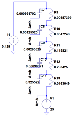
Figure 11. Example of a MOSFET Cauer model with 5 RC networks
RC models can be generated through curve fitting algorithms and mathematical transforms with excellent alignment to transient measurements and calibrated CFD simulations. Further information can be found in application note AN11261 RC Thermal Models [4].
In addition to electrical models, Nexperia has an ever-expanding portfolio of 5-pin Precision Electrothermal Models (PETs) shown in Fig.11. PETs build upon what is offered by standard RC models. These models have two additional pins, revealing junction temperature and mounting base temperature for the user to connect or probe. These models offer improved accuracy over legacy electrical models as the electrical behaviour can change due to MOSFET self-heating.
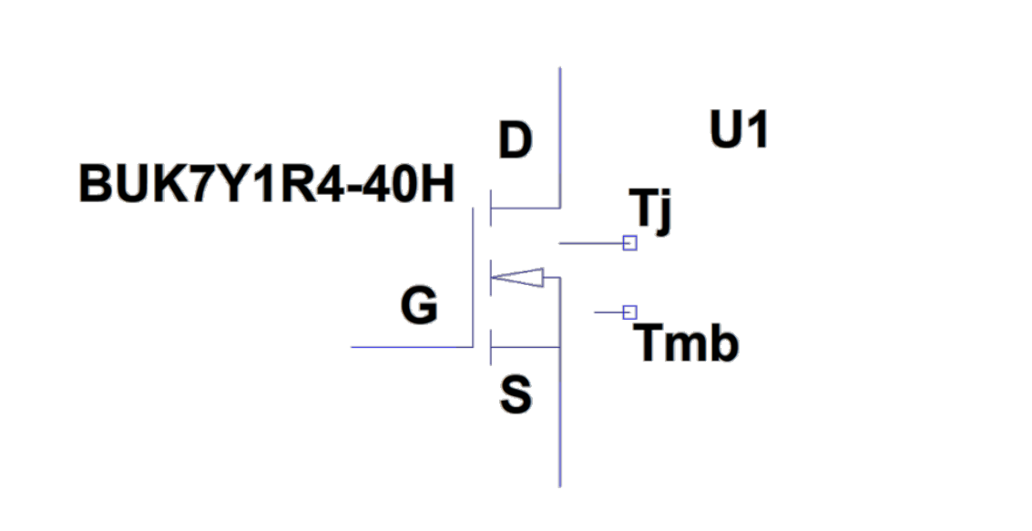
Figure11. Example of a LFPAK56 5-pin Precision Electrothermal Model
4.2. PCB models
As explained previously, heat does not stop at the boundary of a MOSFET and will exit into the PCB and ambient in an application. For a long time due to the complexity and variance of Rth(j-amb), there was no availability of PCB thermal models. Designers would need to estimate a characteristic thermal resistance and thermal capacitance of the PCB to connect in series with the MOSFET RC model to give an estimated steady-state thermal response. Any forced cooling in the system or additional RC networks would be very difficult to estimate given the many environmental variables that can be present.
During this study, Nexperia managed to collate a range of thermal data across all packages from measurements and calibrated CFD simulations. Through the use of curve fitting algorithms and calculations, the mounting base to ambient thermal resistance was able to be derived to create PCB Cauer models. Cauer models were chosen over Foster models, as each node bears physical significance to a position in the model.
Since each node of a Cauer model corresponds to a location within the physical build of the MOSFET and PCB, the position at which Cauer models are connected matters. Hence, PCB Cauer models should be connected after the MOSFET Cauer model. In addition, each MOSFET can only be connected to a single PCB Cauer model as they cannot account for thermal coupling between devices. If there are multiple MOSFETs in a setup, they will each need their own PCB Cauer model. An example of a MOSFET and PCB Cauer connection is shown in Fig. 12

Figure 12. Example of an RC thermal model, with discrete MOSFET and PCB Cauer connected in series
PCB Cauers were created across several package types, substrates and both for constant cooled and natural convection scenarios. The reason why PCB models are package specific is due to the differing rates of heat flow experienced by smaller and larger devices of different mounting base areas, as explained previously with Equation 2. For example, the PCB used for a LFPAK88 device can disspiate more power than an identical substrate used for a LFPAK33.

Figure 13. Comparison between circuit simulation and measurements, showing the steady-state thermal resistance of LFPAK88 on PCBs clamped to a constant cooled cold plate
After their creation, these Cauer models then underwent validation against real measurements in a circuit simulator and from Fig 13, they are seen to bear close resemblance to each other. This demonstrates that the PCB Cauer models are able to provide precise and rapid estimations of MOSFET thermal behaviour. This is a huge advantage and reduces the need for designers to perform physical measurements or complex CFD simulations that either require physical prototypes and heavy computational resources. Nexperia intends to expand the library of PCB Cauer models to cover more PCB types to further aid designers in the future.
7. Summary
This interactive application note has shown the huge variability of the parameter Rth(j-amb) and the challenges faced by design engineers to ensure applications can cope with thermal losses. The study has shown that if a designer is able to decrease the thermal resistance of the PCB through methods such as increasing copper area, thermal vias and using high conductivity materials, smaller MOSFETs can exhibit similar thermal performance to larger MOSFETs under natural convection.
Device level thermal performance is readily available from manufacturers. However, the thermal performance of a MOSFETs can vary hugely in different applications and product designs. This study was initiated with the intent to help designers in their initial design phases where PCB layout and construction is not yet known. The intention was to give users precise thermal estimation tools that are easily accessible and easy to use compared to lengthy measurement and CFD simulation methods.
From this study, Nexperia has managed to create a library of PCB Cauer models across several package types for constant cooled and natural convection scenarios to show the user the variability of thermal performance depending on user design. The results of which aim to streamline the thermal design process and decrease the time taken for designers to create new products. These PCB Cauer models are free to access on Siemens PartQuest along with Nexperia electrical and Precision Electrothermal Models.
A PartQuest embedded Cloud simulation was used in this interactive application note.
References
[1] AN90003, LFPAK MOSFET thermal design guide, Nexperia.
[2] JESD51-14, Transient Dual Interface Test Method for the Measurement of the Thermal Resistance Junction-to-Case of Semiconductor Devices with Heat Flow Through a Single Path, JEDEC SOLID STATE TECHNOLOGY ASSOCIATION.
[3] JESD51-2A, Integrated Circuits Thermal Test Method Environmental Conditions - Natural Convection (Still Air), JEDEC SOLID STATE TECHNOLOGY ASSOCIATION.
[4] AN11261, RC thermal models, Nexperia.
| Page last updated 15 April 2024. |