


74HC574-Q100; 74HCT574-Q100
Octal D-type flip-flop; positive edge-trigger; 3-state
The 74HC574-Q100; 74HCT574-Q100 is an 8-bit positive-edge triggered D-type flip-flop with 3-state outputs. The device features a clock (CP) and output enable (OE) inputs. The flip-flops will store the state of their individual D-inputs that meet the set-up and hold time requirements on the LOW-to-HIGH clock (CP) transition. A HIGH on OE causes the outputs to assume a high-impedance OFF-state. Operation of the OE input does not affect the state of the flip-flops. Inputs include clamp diodes. This enables the use of current limiting resistors to interface inputs to voltages in excess of VCC.
This product has been qualified to the Automotive Electronics Council (AEC) standard Q100 (Grade 1) and is suitable for use in automotive applications.
Features and benefits
Automotive product qualification in accordance with AEC-Q100 (Grade 1)
Specified from -40 °C to +85 °C and from -40 °C to +125 °C
Wide supply voltage range from 2.0 V to 6.0 V
CMOS low power dissipation
High noise immunity
Latch-up performance exceeds 100 mA per JESD 78 Class II Level B
Complies with JEDEC standards:
JESD8C (2.7 V to 3.6 V)
JESD7A (2.0 V to 6.0 V)
Input levels:
For 74HC574-Q100: CMOS level
For 74HCT574-Q100: TTL level
3-state non-inverting outputs for bus oriented applications
8-bit positive, edge-triggered register
Common 3-state output enable input
ESD protection:
HBM: ANSI/ESDA/JEDEC JS-001 class 2 exceeds 2000 V
CDM: ANSI/ESDA/JEDEC JS-002 class C3 exceeds 1000 V
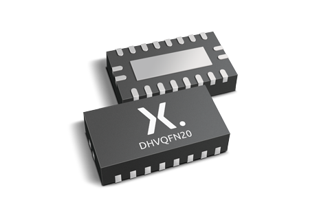
DHVQFN package with Side-Wettable Flanks enabling Automated Optical Inspection (AOI) of solder joints
参数类型
| 型号 | VCC (V) | Logic switching levels | Output drive capability (mA) | tpd (ns) | fmax (MHz) | Power dissipation considerations | Tamb (°C) | Rth(j-a) (K/W) | Ψth(j-top) (K/W) | Rth(j-c) (K/W) | Package name |
|---|---|---|---|---|---|---|---|---|---|---|---|
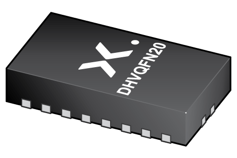
| 74HC574BQ-Q100 | 2.0 - 6.0 | CMOS | ± 7.8 | 14 | 133 | low | -40~125 | 77 | 9.4 | 50 | DHVQFN20 |
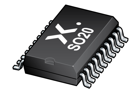
| 74HC574D-Q100 | 2.0 - 6.0 | CMOS | ± 7.8 | 14 | 133 | low | -40~125 | 27.5 | 61 | SO20 | |
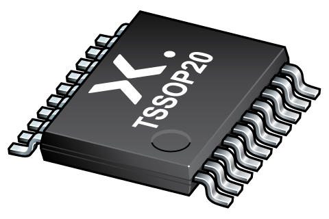
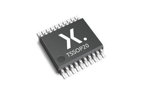
| 74HC574PW-Q100 | 2.0 - 6.0 | CMOS | ± 7.8 | 14 | 133 | low | -40~125 | 4.6 | 44.9 | TSSOP20 | |
| 74HCT574D-Q100 | 4.5 - 5.5 | TTL | ± 6 | 15 | 76 | low | -40~125 | 27.5 | 61 | SO20 | |
| 74HCT574PW-Q100 | 4.5 - 5.5 | TTL | ± 6 | 15 | 76 | low | -40~125 | 4.6 | 44.9 | TSSOP20 |
封装
| 型号 | 可订购的器件编号,(订购码(12NC)) | 状态 | 标示 | 封装 | 外形图 | 回流焊/波峰焊 | 包装 |
|---|---|---|---|---|---|---|---|
| 74HC574BQ-Q100 | 74HC574BQ‑Q100X (935691307115) |
Active | 74HC574B |
DHVQFN20 (SOT764-1) |
SOT764-1 | SOT764-1_115 | |
| 74HC574D-Q100 | 74HC574D‑Q100,118 (935298937118) |
Active | 74HC574D |
SO20 (SOT163-1) |
SOT163-1 |
WAVE_BG-BD-1
|
SOT163-1_118 |
| 74HC574PW-Q100 | 74HC574PW‑Q100,118 (935298938118) |
Active | HC574 |
TSSOP20 (SOT360-1) |
SOT360-1 |
SSOP-TSSOP-VSO-WAVE
|
SOT360-1_118 |
| 74HCT574D-Q100 | 74HCT574D‑Q100,118 (935298939118) |
Active | 74HCT574D |
SO20 (SOT163-1) |
SOT163-1 |
WAVE_BG-BD-1
|
SOT163-1_118 |
| 74HCT574PW-Q100 | 74HCT574PW‑Q100,11 (935298941118) |
Active | HCT574 |
TSSOP20 (SOT360-1) |
SOT360-1 |
SSOP-TSSOP-VSO-WAVE
|
SOT360-1_118 |
环境信息
| 型号 | 可订购的器件编号 | 化学成分 | RoHS | RHF指示符 |
|---|---|---|---|---|
| 74HC574BQ-Q100 | 74HC574BQ‑Q100X | 74HC574BQ-Q100 |
|
|
| 74HC574D-Q100 | 74HC574D‑Q100,118 | 74HC574D-Q100 |
|
|
| 74HC574PW-Q100 | 74HC574PW‑Q100,118 | 74HC574PW-Q100 |
|
|
| 74HCT574D-Q100 | 74HCT574D‑Q100,118 | 74HCT574D-Q100 |
|
|
| 74HCT574PW-Q100 | 74HCT574PW‑Q100,11 | 74HCT574PW-Q100 |
|
|
文档 (15)
| 文件名称 | 标题 | 类型 | 日期 |
|---|---|---|---|
| 74HC_HCT574_Q100 | Octal D-type flip-flop; positive edge-trigger; 3-state | Data sheet | 2024-08-05 |
| AN11044 | Pin FMEA 74HC/74HCT family | Application note | 2019-01-09 |
| AN90063 | Questions about package outline drawings | Application note | 2025-10-22 |
| SOT764-1 | 3D model for products with SOT764-1 package | Design support | 2019-10-03 |
| SOT163-1 | 3D model for products with SOT163-1 package | Design support | 2020-01-22 |
| SOT360-1 | 3D model for products with SOT360-1 package | Design support | 2020-01-22 |
| Nexperia_package_poster | Nexperia package poster | Leaflet | 2020-05-15 |
| DHVQFN20_SOT764-1_mk | plastic, dual in-line compatible thermal enhanced very thin quad flat package; 20 terminals; 0.5 mm pitch; 2.5 mm x 4.5 mm x 0.85 mm body | Marcom graphics | 2017-01-28 |
| TSSOP20_SOT360-1_mk | plastic, thin shrink small outline package; 20 leads; 0.65 mm pitch; 6.5 mm x 4.4 mm x 1.1 mm body | Marcom graphics | 2017-01-28 |
| SOT764-1 | plastic, leadless dual in-line compatible thermal enhanced very thin quad flat package; 20 terminals; 0.5 mm pitch; 4.5 mm x 2.5 mm x 1 mm body | Package information | 2022-06-21 |
| SOT163-1 | plastic, small outline package; 20 leads; 1.27 mm pitch; 12.8 mm x 7.5 mm x 2.65 mm body | Package information | 2024-11-15 |
| SOT360-1 | plastic, thin shrink small outline package; 20 leads; 0.65 mm pitch; 6.5 mm x 4.4 mm x 1.2 mm body | Package information | 2024-11-15 |
| HCT_USER_GUIDE | HC/T User Guide | User manual | 1997-10-31 |
| WAVE_BG-BD-1 | Wave soldering profile | Wave soldering | 2021-09-08 |
| SSOP-TSSOP-VSO-WAVE | Footprint for wave soldering | Wave soldering | 2009-10-08 |
支持
如果您需要设计/技术支持,请告知我们并填写 应答表 我们会尽快回复您。
Ordering, pricing & availability
样品
作为 Nexperia 的客户,您可以通过我们的销售机构订购样品。
如果您没有 Nexperia 的直接账户,我们的全球和地区分销商网络可为您提供 Nexperia 样品支持。查看官方经销商列表。