


HEF4013B-Q100
Dual D-type flip-flop
The HEF4013B-Q100 is a dual D-type flip-flop with set and reset; positive-edge trigger. Inputs include clamp diodes. This enables the use of current limiting resistors to interface inputs to voltages in excess of VDD. Schmitt-trigger action on the clock input makes the circuit highly tolerant of slower clock rise and fall times.
This product has been qualified to the Automotive Electronics Council (AEC) standard Q100 (Grade 1) and is suitable for use in automotive applications.
Features and benefits
Automotive product qualification in accordance with AEC-Q100 (Grade 1)
Specified from -40 °C to +85 °C and from -40 °C to +125 °C
Wide supply voltage range from 3.0 V to 15.0 V
CMOS low power dissipation
High noise immunity
Tolerant of slow clock rise and fall times
Fully static operation
5 V, 10 V, and 15 V parametric ratings
Standardized symmetrical output characteristics
Complies with JEDEC standard JESD 13-B
-
ESD protection:
HBM: ANSI/ESDA/JEDEC JS-001 class 2 exceeds 2000 V
CDM: ANSI/ESDA/JEDEC JS-002 class C3 exceeds 1000 V
Applications
Counters and dividers
Registers
Toggle flip-flops
参数类型
| 型号 | VCC (V) | Logic switching levels | Output drive capability (mA) | tpd (ns) | fmax (MHz) | Power dissipation considerations | Tamb (°C) | Rth(j-a) (K/W) | Ψth(j-top) (K/W) | Rth(j-c) (K/W) | Package name |
|---|---|---|---|---|---|---|---|---|---|---|---|
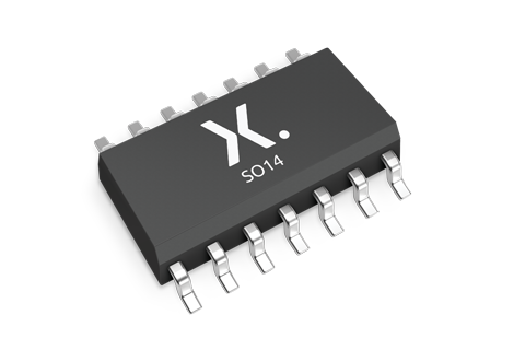
| HEF4013BT-Q100 | 3.0 - 15 | CMOS | ± 2.4 | 30 | 40 | low | -40~125 | 105 | 18.3 | 64 | SO14 |
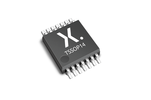
| HEF4013BTT-Q100 | 3.0 - 15 | CMOS | ± 2.4 | 30 | 40 | low | -40~125 | 139 | 7.1 | 65 | TSSOP14 |
封装
| 型号 | 可订购的器件编号,(订购码(12NC)) | 状态 | 标示 | 封装 | 外形图 | 回流焊/波峰焊 | 包装 |
|---|---|---|---|---|---|---|---|
| HEF4013BT-Q100 | HEF4013BT‑Q100J (935299245118) |
Active | HEF4013BT |
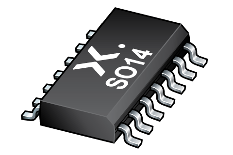
SO14 (SOT108-1) |
SOT108-1 |
SO-SOJ-REFLOW
SO-SOJ-WAVE WAVE_BG-BD-1 |
SOT108-1_118 |
| HEF4013BTT-Q100 | HEF4013BTT‑Q100J (935299246118) |
Active | EF4013B |
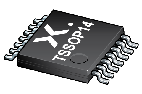
TSSOP14 (SOT402-1) |
SOT402-1 |
SSOP-TSSOP-VSO-WAVE
|
SOT402-1_118 |
环境信息
| 型号 | 可订购的器件编号 | 化学成分 | RoHS | RHF指示符 |
|---|---|---|---|---|
| HEF4013BT-Q100 | HEF4013BT‑Q100J | HEF4013BT-Q100 |
|
|
| HEF4013BTT-Q100 | HEF4013BTT‑Q100J | HEF4013BTT-Q100 |
|
|
文档 (14)
| 文件名称 | 标题 | 类型 | 日期 |
|---|---|---|---|
| HEF4013B_Q100 | Dual D-type flip-flop | Data sheet | 2024-07-24 |
| AN11051 | Pin FMEA HEF4000 family | Application note | 2019-01-09 |
| AN90063 | Questions about package outline drawings | Application note | 2025-10-22 |
| SOT108-1 | 3D model for products with SOT108-1 package | Design support | 2020-01-22 |
| SOT402-1 | 3D model for products with SOT402-1 package | Design support | 2023-02-02 |
| Nexperia_package_poster | Nexperia package poster | Leaflet | 2020-05-15 |
| SO14_SOT108-1_mk | plastic, small outline package; 14 leads; 1.27 mm pitch; 8.65 mm x 3.9 mm x 1.75 mm body | Marcom graphics | 2017-01-28 |
| TSSOP14_SOT402-1_mk | plastic, thin shrink small outline package; 14 leads; 0.65 mm pitch; 5 mm x 4.4 mm x 1.1 mm body | Marcom graphics | 2017-01-28 |
| SOT108-1 | plastic, small outline package; 14 leads; 1.27 mm pitch; 8.65 mm x 3.9 mm x 1.75 mm body | Package information | 2023-11-07 |
| SOT402-1 | plastic, thin shrink small outline package; 14 leads; 0.65 mm pitch; 5 mm x 4.4 mm x 1.2 mm body | Package information | 2023-11-07 |
| SO-SOJ-REFLOW | Footprint for reflow soldering | Reflow soldering | 2009-10-08 |
| SO-SOJ-WAVE | Footprint for wave soldering | Wave soldering | 2009-10-08 |
| WAVE_BG-BD-1 | Wave soldering profile | Wave soldering | 2021-09-08 |
| SSOP-TSSOP-VSO-WAVE | Footprint for wave soldering | Wave soldering | 2009-10-08 |
支持
如果您需要设计/技术支持,请告知我们并填写 应答表 我们会尽快回复您。
Ordering, pricing & availability
样品
作为 Nexperia 的客户,您可以通过我们的销售机构订购样品。
如果您没有 Nexperia 的直接账户,我们的全球和地区分销商网络可为您提供 Nexperia 样品支持。查看官方经销商列表。