


Features and benefits
Low VCEsat (BISS) transistor and resistor-equipped transistor in one package
Low 'threshold' voltage (< 1 V) compared to MOSFET
Low drive power required
Space-saving solution
Reduction of component count
AEC-Q101 qualified
Applications
Supply line switches
Battery charger switches
High-side switches for LEDs, drivers and backlights
Portable equipment
参数类型
| 型号 |
|---|
封装
下表中的所有产品型号均已停产 。
| 型号 | 可订购的器件编号,(订购码(12NC)) | 状态 | 标示 | 封装 | 外形图 | 回流焊/波峰焊 | 包装 |
|---|---|---|---|---|---|---|---|
| PBLS1502V | PBLS1502V,115 (934058048115) |
Obsolete |
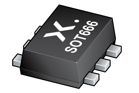
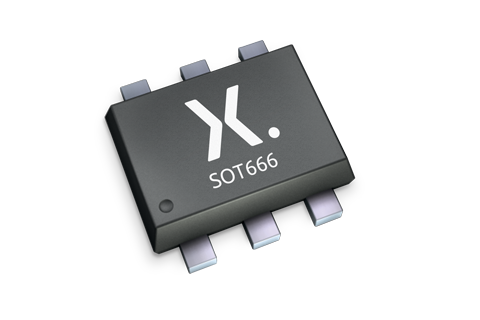
(SOT666) |
SOT666 | SOT666_115 | ||
| PBLS1502Y | PBLS1502Y,115 (934058053115) |
Discontinued / End-of-life | %C2 |
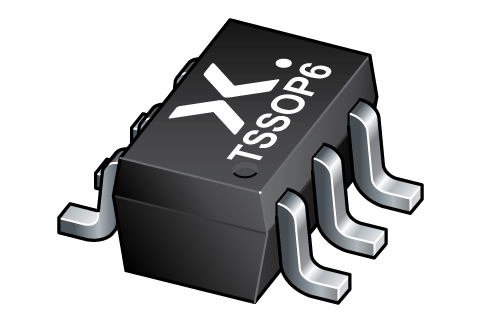
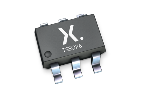
TSSOP6 (SOT363) |
SOT363 |
WAVE_BG-BD-1
|
SOT363_115 |
文档 (16)
| 文件名称 | 标题 | 类型 | 日期 |
|---|---|---|---|
| PBLS1502Y_PBLS1502V | 15 V PNP BISS loadswitch | Data sheet | 2009-09-08 |
| AN90063 | Questions about package outline drawings | Application note | 2025-10-22 |
| AN90032 | Low temperature soldering, application study | Application note | 2022-02-22 |
| 001aab555 | Block diagram: 1PS66SB82, 1PS88SB82, BCM847BS, BCM847BV, BCM847DS, BCM856BS, BCM856DS, BCM857BS, BCM857BV, BCM857DS, PBLS1501V, PBLS1501Y, PBLS1502V, PBLS1502Y, PBLS4001V, PBLS4001Y, PBLS4002V, PBLS4002Y, PBLS4003V, PBLS4003Y, PBLS4004V, PBLS4004Y, PBLS4005V, PBLS4005Y, PBLS1503V, PBLS1503Y, PBLS1504V, PBLS1504Y, PEMD2, PEMH30, PIMD2, PMP4201G, PMP4201V, PMP4201Y, PMP4501G, PMP4501V, PMP4501Y, PMP5201G, PMP5201V, PMP5201Y, PMP5501G, PMP5501V, PMP5501Y, PUMD2, PUMH30 | Block diagram | 2009-11-04 |
| sym036 | Graphic symbol: PNP BISS loadswitch | Block diagram | 2009-11-04 |
| Nexperia_document_guide_MiniLogic_PicoGate_201901 | PicoGate leaded logic portfolio guide | Brochure | 2019-01-07 |
| SOT666 | 3D model for products with SOT666 package | Design support | 2019-01-22 |
| SOT363 | 3D model for products with SOT363 package | Design support | 2018-12-05 |
| Nexperia_package_poster | Nexperia package poster | Leaflet | 2020-05-15 |
| SOT666_mk | plastic, surface-mounted package; 6 leads; 1 mm pitch; 1.6 mm x 1.2 mm x 0.55 mm body | Marcom graphics | 2017-01-28 |
| TSSOP6_SOT363_mk | plastic, surface-mounted package; 6 leads; 1.3 mm pitch; 2 mm x 1.25 mm x 0.95 mm body | Marcom graphics | 2017-01-28 |
| REFLOW_BG-BD-1 | Reflow soldering profile | Other type | 2026-02-10 |
| SOT666 | plastic, surface-mounted package; 6 leads; 0.5 mm pitch; 1.6 mm x 1.2 mm x 0.55 mm body | Package information | 2022-06-01 |
| SOT363 | Plastic surface-mounted package; 6 leads | Package information | 2026-02-16 |
| MAR_SOT363 | MAR_SOT363 Topmark | Top marking | 2013-06-03 |
| WAVE_BG-BD-1 | Wave soldering profile | Wave soldering | 2021-09-08 |
支持
如果您需要设计/技术支持,请告知我们并填写 应答表 我们会尽快回复您。