Orderable parts
| Type number | Orderable part number | Ordering code (12NC) | Package | Buy from distributors |
|---|---|---|---|---|
| NMUX1309APW-Q100 | NMUX1309APW-Q100J | 935692338118 | SOT403-1 | Order product |
Register once, drag and drop ECAD models into your CAD tool and speed up your design.
Click here for more information1.5 V to 5.5 V, dual 4-channel switch analog multiplexer and demultiplexer with injection-current control
The NMUX1309A-Q100 is a general purpose, CMOS, bi-directional, dual 4 channel analog switch, with an operating voltage range of 1.5 V to 5.5 V. The NMUX1309A-Q100 is dual source compatible with existing 4852 and 4052 devices. The NUMX1309A-Q100 extends the digital logic thresholds to be compatible with 1.8 V systems without the need for voltage translation.
The analog signal pins are bi-directional and are comprised of a single common input/output (Z) and eight independent inputs/outputs (Y0 to Y7).
All analog signal pins support overvoltage and undervoltage protection through the integration of injection current control circuitry. This circuit clamps analog signals biased above VCC or biased below GND, saving the need for external overvoltage and undervoltage clamp components (e.g. resistor diode network). This circuit also preserves measurement accuracy of the connected analog signal path by isolating overvoltage events from shifting the device operating voltage.
There are three control signal pins (S0, S1, and E). S0 and S1 determine the analog channels to connect between nZ and nYn. E can be used to override S0 and S1, disconnecting all analog channels. The control signal pins support 1.8 V logic thresholds across all operating voltages. In addition, these pins are 5.5 V tolerant, enabling up to 5.5 V operation independent of supply voltage.
This product has been qualified to the Automotive Electronics Council (AEC) standard Q100 (Grade 1) and is suitable for use in automotive applications.
Automotive product qualification in accordance with AEC-Q100 (Grade 1)
Wide operating range: 1.5 V to 5.5 V
2x SP4T-Z functionality
Rail-to-Rail operation on analog signal pins
Injection current control: 0.1 mV measurement voltage offset up to 10 mA of injected current
Digital pins compatible with 1.8 V logic thresholds across full VCC range
Removes need for up-translation device for compatibility with low voltage GPIOs
Ioff circuitry
Enables wider latitude for power sequencing considerations
Isolates backflow between supply rail and any biased digital/analog input when VCC = 0 V
Prevents any biased digital/analog input from backpowering VCC when VCC = 0 V
Supports switching of 5.5 V digital signals across full VCC operating range
Removes need for down-translation when switching thresholds are met
Pin compatible with industry standard 4052 and 4852 analog switch products
HBM: ANSI/ESDA/JEDEC JS-001 class 2 exceeds 2000 V
CDM: ANSI/ESDA/JEDEC JS-002 class C2b exceeds 750 V
DHVQFN package with Side-Wettable Flanks enabling Automated Optical Inspection (AOI) of solder joints
Body control module
Battery management system
Automotive head unit
| Type number | Configuration | VCC (V) | RON (Ω) | RON(FLAT) (Ω) | Logic switching levels | Power dissipation considerations | Tamb (°C) | Rth(j-a) (K/W) | Ψth(j-top) (K/W) | Rth(j-c) (K/W) | Package name |
|---|---|---|---|---|---|---|---|---|---|---|---|
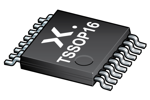
| NMUX1309APW-Q100 | SP4T-Z | 1.5 - 5.5 | 60 | - | CMOS | very low | -40~125 | 139 | 64 | 6.9 | TSSOP16 |
| Type number | Orderable part number, (Ordering code (12NC)) | Status | Marking | Package | Package information | Reflow-/Wave soldering | Packing |
|---|---|---|---|---|---|---|---|
| NMUX1309APW-Q100 | NMUX1309APW-Q100J (935692338118) |
Active | NM1309A |
TSSOP16 (SOT403-1) |
SOT403-1 |
SSOP-TSSOP-VSO-WAVE
|
SOT403-1_118 |
| Type number | Orderable part number | Chemical content | RoHS | RHF-indicator |
|---|---|---|---|---|
| NMUX1309APW-Q100 | NMUX1309APW-Q100J | NMUX1309APW-Q100 |
|
|
| File name | Title | Type | Date |
|---|---|---|---|
| NMUX1309A_Q100 | 1.5 V to 5.5 V, dual 4-channel switch analog multiplexer and demultiplexer with injection-current control | Data sheet | 2025-05-16 |
| AN90062 | Analog multiplexers and switches | Application note | 2025-05-15 |
| AN90063 | Questions about package outline drawings | Application note | 2025-06-13 |
| SOT403-1 | 3D model for products with SOT403-1 package | Design support | 2020-01-22 |
| Nexperia_package_poster | Nexperia package poster | Leaflet | 2020-05-15 |
| TSSOP16_SOT403-1_mk | plastic, thin shrink small outline package; 16 leads; 0.65 mm pitch; 5 mm x 4.4 mm x 1.1 mm body | Marcom graphics | 2017-01-28 |
| SOT403-1 | plastic, thin shrink small outline package; 16 leads; 5 mm x 4.4 mm x 1.2 mm body | Package information | 2023-11-08 |
| SOT403-1_118 | TSSOP16; Reel pack for SMD, 13"; Q1/T1 product orientation | Packing information | 2020-04-21 |
| UM90066 | User Guide for NEVB-NMUXGP1 Evaluation Board | User manual | 2025-07-17 |
| SSOP-TSSOP-VSO-WAVE | Footprint for wave soldering | Wave soldering | 2009-10-08 |
If you are in need of design/technical support, let us know and fill in the answer form we'll get back to you shortly.
The Nexperia Longevity Program is aimed to provide our customers information from time to time about the expected time that our products can be ordered. The NLP is reviewed and updated regularly by our Executive Management Team. View our longevity program here.
| File name | Title | Type | Date |
|---|---|---|---|
| SOT403-1 | 3D model for products with SOT403-1 package | Design support | 2020-01-22 |
| Type number | Orderable part number | Ordering code (12NC) | Status | Packing | Packing Quantity | Buy online |
|---|---|---|---|---|---|---|
| NMUX1309APW-Q100 | NMUX1309APW-Q100J | 935692338118 | Active | SOT403-1_118 | 2,500 |
|
As a Nexperia customer you can order samples via our sales organization.
If you do not have a direct account with Nexperia our network of global and regional distributors is available and equipped to support you with Nexperia samples. Check out the list of official distributors.
The interactive datasheets are based on the Nexperia MOSFET precision electrothermal models. With our interactive datasheets you can simply specify your own conditions interactively. Start by changing the values of the conditions. You can do this by using the sliders in the condition fields. By dragging the sliders you will see how the MOSFET will perform at the new conditions set.