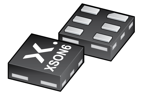
可订购部件
| 型号 | 可订购的器件编号 | 订购代码(12NC) | 封装 | 从经销商处购买 |
|---|---|---|---|---|
| NXB0101GS-Q100 | NXB0101GS-Q100H | 935691515125 | SOT1202 | 订单产品 |

Register once, drag and drop ECAD models into your CAD tool and speed up your design.
Click here for more informationDual supply translating transceiver; auto direction sensing; 3-state
The NXB0101-Q100 is a 1-bit, dual supply translating transceiver with auto direction sensing, that enables bidirectional voltage level translation. It features two 1-bit input-output ports (A and B), one output enable input (OE) and two supply pins (VCC(A) and VCC(B)). VCC(A) can be supplied at any voltage between 1.2 V and 3.6 V and VCC(B) can be supplied at any voltage between 1.65 V and 5.5 V, making the device suitable for translating between any of the low voltage nodes (1.2 V, 1.5 V, 1.8 V, 2.5 V, 3.3 V and 5.0 V). Pin A and OE are referenced to VCC(A) and pins B is referenced to VCC(B). A LOW level at pin OE causes the outputs to assume a high-impedance OFF-state. This device is fully specified for partial power-down applications using IOFF. The IOFF circuitry disables the output, preventing the damaging backflow current through the device when it is powered down.
This product has been qualified to the Automotive Electronics Council (AEC) standard Q100 (Grade 1) and is suitable for use in automotive applications.
Automotive product qualification in accordance with AEC-Q100 (Grade 1)
Specified from -40 °C to +85 °C and from -40 °C to +125 °C
Wide supply voltage range:
VCC(A): 1.2 V to 3.6 V and VCC(B): 1.65 V to 5.5 V
IOFF circuitry provides partial Power-down mode operation
Inputs accept voltages up to 5.5 V
ESD protection:
HBM: ANSI/ESDA/JEDEC JS-001 class 2 exceeds 2500 V for A port
HBM: ANSI/ESDA/JEDEC JS-001 class 3B exceeds 15000 V for B port
CDM: ANSI/ESDA/JEDEC JS-002 class C3 exceeds 1500 V
Latch-up performance exceeds 100 mA per JESD 78B Class II
| 型号 | VCC (V) | Logic switching levels | Output drive capability (mA) | Nr of bits | Power dissipation considerations | Tamb (°C) | Package name |
|---|---|---|---|---|---|---|---|
| NXB0101GS-Q100 | n.a. | CMOS | ± 0.02 | 1 | low | -40~125 | XSON6 |
| 型号 | 可订购的器件编号,(订购码(12NC)) | 状态 | 标示 | 封装 | 外形图 | 回流焊/波峰焊 | 包装 |
|---|---|---|---|---|---|---|---|
| NXB0101GS-Q100 | NXB0101GS-Q100H (935691515125) |
Active | n1 |

XSON6 (SOT1202) |
SOT1202 |
REFLOW_BG-BD-1
|
暂无信息 |
| 文件名称 | 标题 | 类型 | 日期 |
|---|---|---|---|
| NXB0101_Q100 | Dual supply translating transceiver; auto direction sensing; 3-state | Data sheet | 2023-11-15 |
| Nexperia_document_guide_MiniLogic_MicroPak_201808 | MicroPak leadless logic portfolio guide | Brochure | 2018-09-03 |
| SOT1202 | 3D model for products with SOT1202 package | Design support | 2023-02-02 |
| Nexperia_package_poster | Nexperia package poster | Leaflet | 2020-05-15 |
| SOT1202 | plastic, leadless extremely thin small outline package; 6 terminals; 0.35 mm pitch; 1 mm x 1mm x 0.35 mm body | Package information | 2022-06-01 |
| NXB0101GS-Q100_Nexperia_Product_Reliability | NXB0101GS-Q100 Nexperia Product Reliability | Quality document | 2024-06-16 |
| REFLOW_BG-BD-1 | Reflow soldering profile | Reflow soldering | 2021-04-06 |
| MAR_SOT1202 | MAR_SOT1202 Topmark | Top marking | 2013-06-03 |
如果您需要设计/技术支持,请告知我们并填写 应答表 我们会尽快回复您。
| 文件名称 | 标题 | 类型 | 日期 |
|---|---|---|---|
| SOT1202 | 3D model for products with SOT1202 package | Design support | 2023-02-02 |
| 型号 | Orderable part number | Ordering code (12NC) | 状态 | 包装 | Packing Quantity | 在线购买 |
|---|---|---|---|---|---|---|
| NXB0101GS-Q100 | NXB0101GS-Q100H | 935691515125 | Active | 暂无信息 | 5,000 | 订单产品 |
作为 Nexperia 的客户,您可以通过我们的销售机构订购样品。
如果您没有 Nexperia 的直接账户,我们的全球和地区分销商网络可为您提供 Nexperia 样品支持。查看官方经销商列表。
The interactive datasheets are based on the Nexperia MOSFET precision electrothermal models. With our interactive datasheets you can simply specify your own conditions interactively. Start by changing the values of the conditions. You can do this by using the sliders in the condition fields. By dragging the sliders you will see how the MOSFET will perform at the new conditions set.