

Nexperia expands GaN portfolio with ultra-low-resistance devices for next-generation power density and efficiency
十一月 10, 2026Nijmegen -- New 18 V to 200 V GaN devices offer RDS(on) down to 0.32 mΩ in compact thermally enhanced packages for robotics, AI and renewable energy.

Nexperia today announced new ultra-low-ohmic gallium nitride (GaN) FETs, expanding its low- and medium-voltage GaN portfolio with devices spanning 18 V to 200 V. Designed to address power design challenges in AI datacentres, humanoid robotics, battery-powered tools, renewable energy, high-efficiency SR and DC-DC conversion, the new devices combine high current capability, fast switching performance and compact thermally enhanced packages to support increased efficiency and power density across a broad range of applications.
The new family leverages industry-leading GaN technology to achieve record-low on-state resistance, with sub-milliohm RDS(on) in a PCB footprint of 10 mm². Combined with low RDS(on) × QG and RDS(on) × QOSS figures of merit, these devices support higher switching frequencies and reduced switching losses in demanding power conversion applications. These characteristics are particularly relevant for next-generation power systems, where increasing demands for efficiency, power density and compact form factors are driving the adoption of advanced DC-DC converter topologies and high-performance three-phase BLDC/PMSM motor drives.
In high-density DC-DC power conversion, the medium-voltage 100 V to 200 V portfolio addresses both primary-side and secondary-side power stages in isolated topologies, as well as non-isolated step-down converters. These devices are ideally suited for half-bridge and full-bridge LLC resonant converters, while also enabling highly efficient synchronous rectification in 48 V power-delivery architectures increasingly used in AI infrastructure.
The low-voltage 18 V to 40 V devices are optimised for secondary-side synchronous rectification and low-voltage power-distribution stages, enabling efficient conversion from 12 V rails down to sub-1 V processor core voltages.
In motion control applications, the combination of low RDS(on) and compact package dimensions enables high current capability within a small PCB footprint. Fast switching performance supports efficient inverter operation, optimised dead-time control and, where required, 100% duty-cycle operation. Together, these capabilities enable advanced modulation techniques that improve current control, thermal performance and overall system efficiency.
“The introduction of these new GaN-based solutions marks an important milestone in Nexperia’s journey to becoming a leader in wide-bandgap power semiconductors,” said Andrea Bricconi, Vice President and Head of the GaN Product Group. “From AI datacentres to humanoid robotics, next-generation systems demand ever higher levels of efficiency, performance and power density. This new portfolio reinforces Nexperia’s role in enabling the power architectures that will support these rapidly evolving applications.”
“AI datacentres are driving unprecedented demand for efficiency and power density, accelerating the adoption of highly efficient power conversion architectures that step down from 800 VDC to 48 VDC, 12 VDC and even 6 VDC,” said Roberto Crisafulli, Director of GaN Marketing and Applications. “Our new low- and medium-voltage GaN products are foundational building blocks for advanced multi-level and stacked power conversion architectures, enabling the efficiency, scalability and power density required by next-generation AI power delivery systems.”
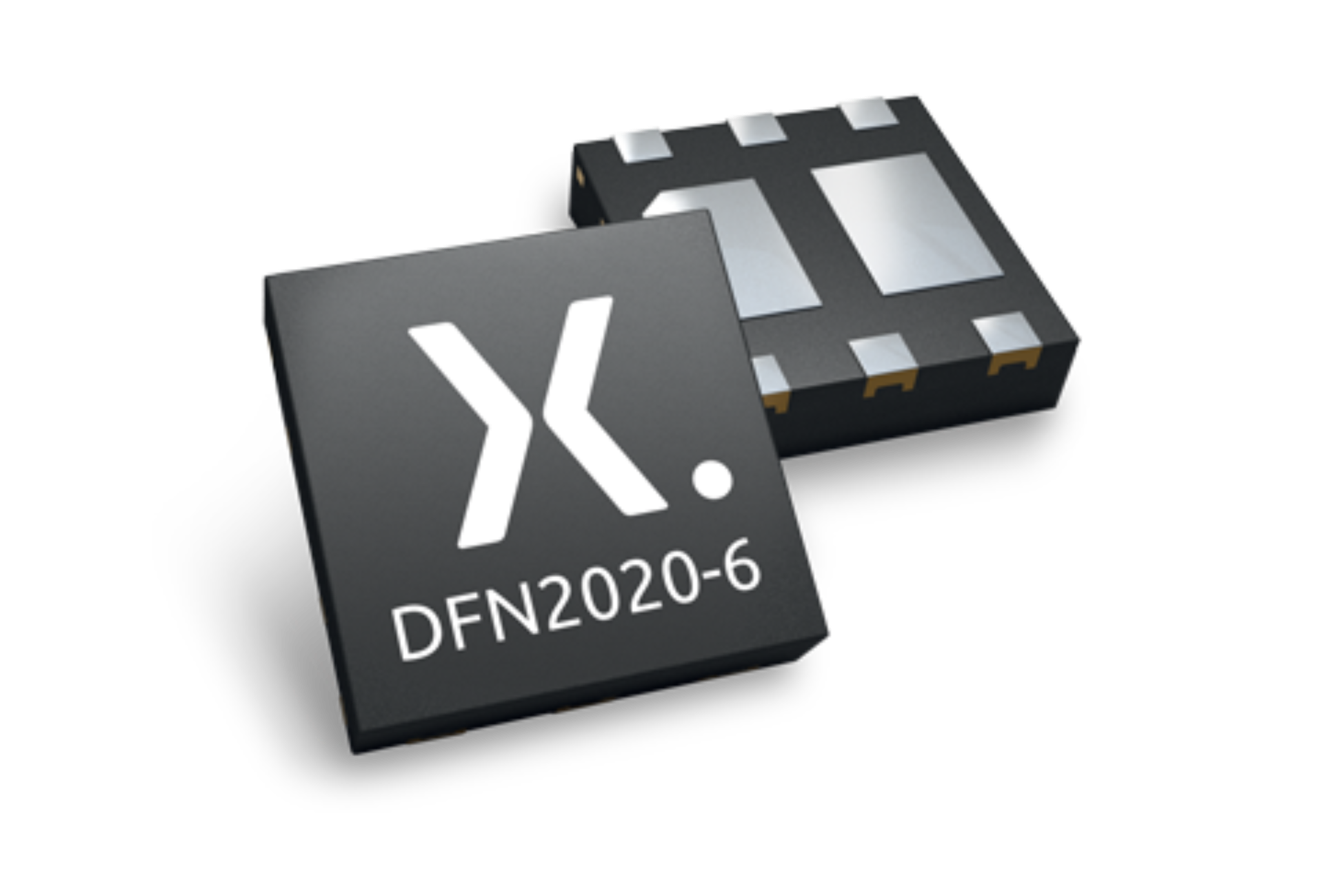
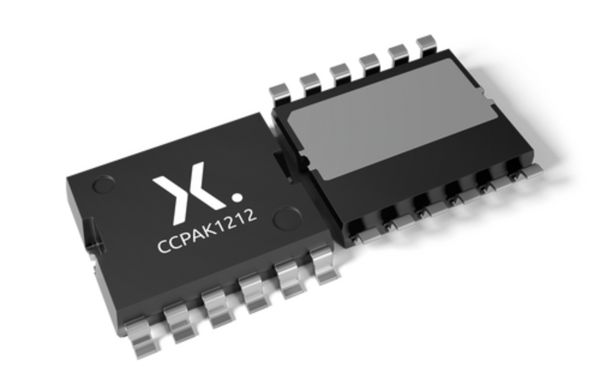
The flagship product in the series, the GANE0R8-100QTM, a 100 V GaN FET featuring a typical RDS(on) of just 0.75 mΩ in a compact 3 mm × 5 mm PQFN package, is available now alongside five additional portfolio members spanning 25 V to 200 V and offering RDS(on) values down to 0.37 mΩ. Two further devices, including the 18 V GANE0R3-015QTL with a typical RDS(on) of 0.32 mΩ, are scheduled for release in Q1 2027, completing a portfolio of eight products spanning 18 V to 200 V. The family ranges from a 18 V device in a 3.3 mm × 3.3 mm PQFN package to a 200 V device in a 3 mm × 5 mm PQFN package, with both package options incorporating an exposed pad designed to support top-side cooling and improved thermal performance.
Learn more about Nexperia’s low-voltage GaN FETs and medium-voltage GaN FETs at nexperia.com.
About Nexperia
Headquartered in the Netherlands, Nexperia is a global semiconductor company with a rich European history and over 10,000 employees across Europe, Asia, and the United States. As a leading expert in the development and production of essential semiconductors, Nexperia’s components enable the basic functionality of virtually every commercial electronic design in the world – from automotive and industrial to mobile and consumer applications.
The company serves a global customer base, shipping around 100 billion products annually. These products are recognized as benchmarks in efficiency – in process, size, power, and performance. Nexperia's commitment to innovation, efficiency, sustainability, and stringent industry requirements is evident in its extensive IP portfolio, its expanding product range, and its certification to IATF 16949, ISO 9001, ISO 14001 and ISO 45001 standards.
For press information, please contact:
Nexperia
Anne Proch
Tel: +49 160 916 884 18
Email: anne.proch@nexperia.com
Pretzl Group
Lucy Sorton
Tel: +44 07966 301949
E-mail: lucy.sorton@pretzl.com