


.png
)
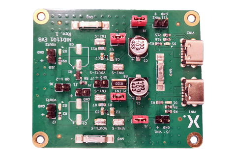
NEVB-NID1101 - 1.5-5.5 V, 1.5 A forward voltage blocking ideal diode evaluation board
The NEVB-NID1101 evaluation PCB incorporates two NID1101 ideal diodes, enabling the assessment of performance and behavior across various use cases, such as OR-ing, power supply multiplexing, and parallel operation. NEVB-NID1101 offers convenient access to multiple power supply inputs, as well as probe hook-ups for evaluation. Additionally, it includes an NMOS transistor at the output to test short circuit behavior.
NEVB-NID1101
.jpg)
Key features & benefits
- Input operating voltage range (VIN): 1.5 V to 5.5 V
- Continuous output current: 1.5 A
- Two supply inputs (VIN1, VIN2)
- Two optional USB-C supply inputs for VIN1 and VIN2
- Access to all device pins
- Use case selection by means of jumpers
- Short circuit testing

相关板块 (1)
| Board | Description | Type | Quick links | Shop link | |
|---|---|---|---|---|---|
|
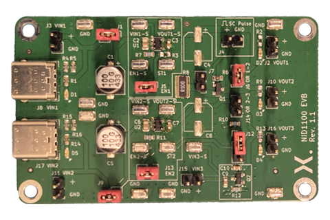
NEVB-NID1100---1-5-5-5-V---1-A-forward-voltage-blocking-ideal-diode-evaluation-board | NEVB-NID1100 - 1.5-5.5 V , 1 A forward voltage blocking ideal diode evaluation board | Evaluation board | 订单 |
相关板块 (1)
| Board | Description | Type | Quick links | Shop link | |
|---|---|---|---|---|---|
|
|
NEVB-NID1100---1-5-5-5-V---1-A-forward-voltage-blocking-ideal-diode-evaluation-board | NEVB-NID1100 - 1.5-5.5 V , 1 A forward voltage blocking ideal diode evaluation board | Evaluation board | 订单 |
文档 (1)
| 文件名称 | 标题 | 类型 | 日期 |
|---|---|---|---|
| UM90071 | NEVB-NID1101 Evaluation board user manual | User manual | 2025-10-10 |