


74ALVCH16646
16-bit bus transceiver/register; 3-state
The 74ALVCH16646 consists of 16 non-inverting bus transceiver circuits with 3-state outputs, D-type flip-flops and control circuitry arranged for multiplexed transmission of data directly from the internal registers. Data on the ‘A’ or ‘B’ bus will be clocked in the internal registers, as the appropriate clock (nCPAB or nCPBA) goes to a HIGH logic level. Output enable (nOE) and direction (nDIR) inputs are provided to control the transceiver function. In the transceiver mode, data present at the high-impedance port may be stored in either the ‘A’ or ‘B’ register, or in both. The select source inputs (nSAB and nSBA) can multiplex stored and real-time (transparent mode) data. The direction (nDIR) input determines which bus will receive data when nOE is active (LOW). In the isolation mode (nOE = HIGH), ‘A’ data may be stored in the ‘B’ register and/or ‘B’ data may be stored in the ‘A’ register.
When an output function is disabled, the input function is still enabled and may be used to store and transmit data. Only one of the two buses, ‘A’ or ‘B’ may be driven at a time.
To ensure the high impedance state during power up or power down, nOE should be tied to VCC through a pullup resistor; the minimum value of the resistor is determined by the current-sinking/current-sourcing capability of the driver.
Active bus-hold circuitry is provided to hold unused or floating data inputs at a valid logic level.
Features and benefits
Wide supply voltage range of 2.3 V to 3.6 V
CMOS low power consumption
MULTIBYTE™ flow-through standard pin-out architecture
Low inductance multiple VCC and GND pins for minimize noise and ground bounce
Bushold on all data inputs
Current drive ±24 mA at VCC = 3.0 V.
Direct interface with TTL levels
Output drive capability 50 Ω transmission lines at 85 °C
Complies with JEDEC standards:
JESD8-7 (1.65 V to 1.95 V)
JESD8-5 (2.3 V to 2.7 V)
JESD8C/JESD36 (2.7 V to 3.6 V)
ESD protection:
- HBM: ANSI/ESDA/JEDEC JS-001 class 2 exceeds 2000 V
- CDM: ANSI/ESDA/JEDEC JS-002 class C3 exceeds 1000 V
Specified from -40 °C to +85 °C
参数类型
| 型号 | VCC(A) (V) | VCC(B) (V) | Logic switching levels | Output drive capability (mA) | tpd (ns) | Nr of bits | fmax (MHz) | Power dissipation considerations | Tamb (°C) | Rth(j-a) (K/W) | Package name |
|---|---|---|---|---|---|---|---|---|---|---|---|
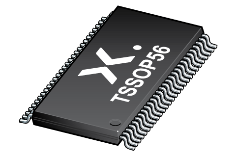
| 74ALVCH16646DGG | n.a. | n.a. | TTL | ± 24 | 2.6 | 16 | 150 | low | -40~85 | 93 | TSSOP56 |
封装
| 型号 | 可订购的器件编号,(订购码(12NC)) | 状态 | 标示 | 封装 | 外形图 | 回流焊/波峰焊 | 包装 |
|---|---|---|---|---|---|---|---|
| 74ALVCH16646DGG | 74ALVCH16646DGG:11 (935262421118) |
Active | ALVCH16646 |

TSSOP56 (SOT364-1) |
SOT364-1 |
SSOP-TSSOP-VSO-WAVE
|
SOT364-1_118 |
文档 (8)
| 文件名称 | 标题 | 类型 | 日期 |
|---|---|---|---|
| 74ALVCH16646 | 16-bit bus transceiver/register; 3-state | Data sheet | 2024-07-05 |
| AN90063 | Questions about package outline drawings | Application note | 2026-06-17 |
| sy00012 | Application diagram: 74LV family, load circuitry for switching times | Block diagram | 2009-11-04 |
| SOT364-1 | 3D model for products with SOT364-1 package | Design support | 2020-01-22 |
| alvch16646 | alvch16646 IBIS model | IBIS model | 2013-04-08 |
| Nexperia_package_poster | Nexperia package poster | Leaflet | 2020-05-15 |
| SOT364-1 | plastic, thin shrink small outline package; 56 leads; 0.5 mm pitch; 14 mm x 6.1 mm x 1.2 mm body | Package information | 2022-06-23 |
| SSOP-TSSOP-VSO-WAVE | Footprint for wave soldering | Wave soldering | 2009-10-08 |
支持
如果您需要设计/技术支持,请告知我们并填写 应答表 我们会尽快回复您。
模型
| 文件名称 | 标题 | 类型 | 日期 |
|---|---|---|---|
| SOT364-1 | 3D model for products with SOT364-1 package | Design support | 2020-01-22 |
| alvch16646 | alvch16646 IBIS model | IBIS model | 2013-04-08 |
Ordering, pricing & availability
样品
作为 Nexperia 的客户,您可以通过我们的销售机构订购样品。
如果您没有 Nexperia 的直接账户,我们的全球和地区分销商网络可为您提供 Nexperia 样品支持。查看官方经销商列表。