


74LV7032A
Quad 2-input OR gate with Schmitt trigger inputs
The 74LV7032A is a quad 2-input OR function with Schmitt-trigger inputs, capable of transforming slowly changing input signals into sharply defined, jitter-free output signals.
Inputs are overvoltage tolerant. This feature allows the use of these devices as translators in mixed voltage environments.
This device is fully specified for partial power down applications using IOFF. The IOFF circuitry disables the output, preventing the potentially damaging backflow current through the device when it is powered down.
Features and benefits
Wide supply voltage range from 2.0 V to 5.5 V
Maximum tpd of 9.5 ns at 5 V
Typical VOL(p) < 0.8 V at VCC = 3.3 V, Tamb = 25 °C
Typical VOH(v) > 2.3 V at VCC = 3.3 V, Tamb = 25 °C
Supports mixed-mode voltage operation on all ports
IOFF circuitry provides partial Power-down mode operation
Latch-up performance exceeds 250 mA per JESD 78 Class II
ESD protection:
HBM: ANSI/ESDA/JEDEC JS-001 class 2 exceeds 2000 V
CDM: ANSI/ESDA/JEDEC JS-002 class C3 exceeds 1000 V
Specified from -40 °C to +85 °C and from -40 °C to +125 °C
参数类型
| 型号 | VCC (V) | Logic switching levels | Output drive capability (mA) | tpd (ns) | fmax (MHz) | Nr of bits | Power dissipation considerations | Tamb (°C) | Rth(j-a) (K/W) | Ψth(j-top) (K/W) | Rth(j-c) (K/W) | Package name |
|---|---|---|---|---|---|---|---|---|---|---|---|---|
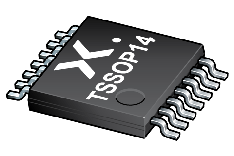
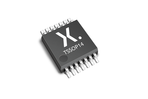
| 74LV7032APW | 2.0 - 5.5 | CMOS | ± 12 | 4.3 | 45 | 4 | low | -40~125 | 140 | 7.5 | 66 | TSSOP14 |
封装
| 型号 | 可订购的器件编号,(订购码(12NC)) | 状态 | 标示 | 封装 | 外形图 | 回流焊/波峰焊 | 包装 |
|---|---|---|---|---|---|---|---|
| 74LV7032APW | 74LV7032APWJ (935690649118) |
Active | LV7032A |

TSSOP14 (SOT402-1) |
SOT402-1 |
SSOP-TSSOP-VSO-WAVE
|
SOT402-1_118 |
文档 (9)
| 文件名称 | 标题 | 类型 | 日期 |
|---|---|---|---|
| 74LV7032A | Quad 2-input OR gate with Schmitt trigger inputs | Data sheet | 2024-04-08 |
| AN90063 | Questions about package outline drawings | Application note | 2026-06-17 |
| SOT402-1 | 3D model for products with SOT402-1 package | Design support | 2023-02-02 |
| lv7032a | 74LV7032A IBIS model | IBIS model | 2019-01-08 |
| Nexperia_document_leaflet_Logic_LV-AT_201903 | LV-A(T) logic family | Leaflet | 2019-03-19 |
| Nexperia_package_poster | Nexperia package poster | Leaflet | 2020-05-15 |
| TSSOP14_SOT402-1_mk | plastic, thin shrink small outline package; 14 leads; 0.65 mm pitch; 5 mm x 4.4 mm x 1.1 mm body | Marcom graphics | 2017-01-28 |
| SOT402-1 | plastic, thin shrink small outline package; 14 leads; 0.65 mm pitch; 5 mm x 4.4 mm x 1.2 mm body | Package information | 2023-11-07 |
| SSOP-TSSOP-VSO-WAVE | Footprint for wave soldering | Wave soldering | 2009-10-08 |
支持
如果您需要设计/技术支持,请告知我们并填写 应答表 我们会尽快回复您。
Ordering, pricing & availability
样品
作为 Nexperia 的客户,您可以通过我们的销售机构订购样品。
如果您没有 Nexperia 的直接账户,我们的全球和地区分销商网络可为您提供 Nexperia 样品支持。查看官方经销商列表。