


74LVC1T45-Q100; 74LVCH1T45-Q100
Dual supply translating transceiver; 3-state
The 74LVC1T45-Q100; 74LVCH1T45-Q100 are single bit, dual supply transceivers with 3-state outputs that enable bidirectional level translation. They feature two 1-bit input-output ports (A and B), a direction control input (DIR) and dual supply pins (VCC(A) and VCC(B)). Both VCC(A) and VCC(B) can be supplied with any voltage between 1.2 V and 5.5 V. This flexibility makes the device suitable for translating between any of the low voltage nodes (1.2 V, 1.5 V, 1.8 V, 2.5 V, 3.3 V and 5.0 V). Pins A and DIR are referenced to VCC(A) and pin B is referenced to VCC(B). A HIGH on DIR allows transmission from A to B and a LOW on DIR allows transmission from B to A.
The devices are fully specified for partial power-down applications using IOFF. The IOFF circuitry disables the output, preventing any damaging backflow current through the device when it is powered down. In suspend mode when either VCC(A) or VCC(B) are at GND level, both A port and B port are in the high-impedance OFF-state.
Active bus hold circuitry in the 74LVCH1T45-Q100 holds unused or floating data inputs at a valid logic level.
This product has been qualified to the Automotive Electronics Council (AEC) standard Q100 (Grade 1) and is suitable for use in automotive applications.
Features and benefits
Automotive product qualification in accordance with AEC-Q100 (Grade 1)
Specified from -40 °C to +85 °C and from -40 °C to +125 °C
Wide supply voltage range:
VCC(A): 1.2 V to 5.5 V
VCC(B): 1.2 V to 5.5 V
High noise immunity
Maximum data rates:
420 Mbps (3.3 V to 5.0 V translation)
210 Mbps (translate to 3.3 V))
140 Mbps (translate to 2.5 V)
75 Mbps (translate to 1.8 V)
60 Mbps (translate to 1.5 V)
Suspend mode
Latch-up performance exceeds 100 mA per JESD 78 Class II
±24 mA output drive (VCC = 3.0 V)
Inputs accept voltages up to 5.5 V
Low power consumption: 16 μA maximum ICC
IOFF circuitry provides partial Power-down mode operation
Complies with JEDEC standards:
JESD8-7 (1.2 V to 1.95 V)
JESD8-5 (1.8 V to 2.7 V)
JESD8C (2.7 V to 3.6 V)
JESD36 (4.5 V to 5.5 V)
ESD protection:
HBM: ANSI/ESDA/JEDEC JS-001 class 3A exceeds 4000 V
CDM: ANSI/ESDA/JEDEC JS-002 class C3 exceeds 1000 V
参数类型
| 型号 | VCC(A) (V) | VCC(B) (V) | Logic switching levels | Output drive capability (mA) | tpd (ns) | Nr of bits | Power dissipation considerations | Tamb (°C) | Rth(j-a) (K/W) | Ψth(j-top) (K/W) | Rth(j-c) (K/W) | Package name |
|---|---|---|---|---|---|---|---|---|---|---|---|---|
| 74LVC1T45GM-Q100 | 1.2 - 5.5 | 1.2 - 5.5 | CMOS/LVTTL | ± 24 | 2.5 | 1 | low | -40~125 | 294 | 6.8 | 147 | XSON6 |
| 74LVC1T45GW-Q100 | 1.2 - 5.5 | 1.2 - 5.5 | CMOS/LVTTL | ± 24 | 2.5 | 1 | low | -40~125 | 268 | 41.4 | 156 | TSSOP6 |
| 74LVCH1T45GW-Q100 | 1.2 - 5.5 | 1.2 - 5.5 | CMOS/LVTTL | ± 24 | 2.5 | 1 | low | -40~125 | 268 | 41.4 | 156 | TSSOP6 |
封装
| 型号 | 可订购的器件编号,(订购码(12NC)) | 状态 | 标示 | 封装 | 外形图 | 回流焊/波峰焊 | 包装 |
|---|---|---|---|---|---|---|---|
| 74LVC1T45GM-Q100 | 74LVC1T45GM‑Q100X (935690846115) |
Active | V5 |

XSON6 (SOT886) |
SOT886 | SOT886_115 | |
| 74LVC1T45GW-Q100 | 74LVC1T45GW‑Q100H (935300935125) |
Active | V5 |

TSSOP6 (SOT363-2) |
SOT363-2 | SOT363-2_125 | |
| 74LVCH1T45GW-Q100 | 74LVCH1T45GW‑Q100H (935300936125) |
Active | X5 |
TSSOP6 (SOT363-2) |
SOT363-2 | SOT363-2_125 |
环境信息
| 型号 | 可订购的器件编号 | 化学成分 | RoHS | RHF指示符 |
|---|---|---|---|---|
| 74LVC1T45GM-Q100 | 74LVC1T45GM‑Q100X | 74LVC1T45GM-Q100 |
|
|
| 74LVC1T45GW-Q100 | 74LVC1T45GW‑Q100H | 74LVC1T45GW-Q100 |
|
|
| 74LVCH1T45GW-Q100 | 74LVCH1T45GW‑Q100H | 74LVCH1T45GW-Q100 |
|
|
文档 (17)
| 文件名称 | 标题 | 类型 | 日期 |
|---|---|---|---|
| 74LVC_LVCH1T45_Q100 | Dual supply translating transceiver; 3-state | Data sheet | 2023-08-04 |
| AN10161 | PicoGate Logic footprints | Application note | 2002-10-29 |
| AN11009 | Pin FMEA for LVC family | Application note | 2019-01-09 |
| AN90063 | Questions about package outline drawings | Application note | 2026-06-17 |
| Nexperia_document_guide_MiniLogic_MicroPak_201808 | MicroPak leadless logic portfolio guide | Brochure | 2018-09-03 |
| SOT886 | 3D model for products with SOT886 package | Design support | 2019-10-03 |
| SOT363-2 | 3D model for products with SOT363-2 package | Design support | 2023-02-02 |
| lvc1t45 | lvc1t45 IBIS model | IBIS model | 2013-04-08 |
| lvch1t45 | lvch1t45 IBIS model | IBIS model | 2013-04-09 |
| Nexperia_document_leaflet_Logic_Automotive_MicroPak_solutions_201904 | Automotive logic in MicroPak leadless packages | Leaflet | 2019-04-18 |
| Nexperia_package_poster | Nexperia package poster | Leaflet | 2020-05-15 |
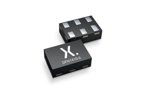
| DFN1410-6_SOT886_mk | plastic, extremely thin small outline package; no leads; 6 terminals; 0.6 mm pitch; 1 mm x 1.45 mm x 0.5 mm body | Marcom graphics | 2017-01-28 |
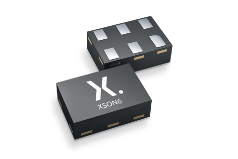
| XSON6_SOT886_mk | plastic, extremely thin small outline package; no leads; 6 terminals; 0.6 mm pitch; 1 mm x 1.45 mm x 0.5 mm body | Marcom graphics | 2017-01-28 |
| REFLOW_BG-BD-1 | Reflow soldering profile | Other type | 2026-02-10 |
| SOT886 | plastic, leadless extremely thin small outline package; 6 terminals; 0.5 mm pitch; 1 mm x 1.45 mm x 0.5 mm body | Package information | 2022-06-01 |
| SOT363-2 | plastic thin shrink small outline package; 6 leads; body width 1.25 mm | Package information | 2022-11-21 |
| MAR_SOT886 | MAR_SOT886 Topmark | Top marking | 2013-06-03 |
支持
如果您需要设计/技术支持,请告知我们并填写 应答表 我们会尽快回复您。
Ordering, pricing & availability
样品
作为 Nexperia 的客户,您可以通过我们的销售机构订购样品。
如果您没有 Nexperia 的直接账户,我们的全球和地区分销商网络可为您提供 Nexperia 样品支持。查看官方经销商列表。