


74AUP2G241
Low-power dual buffer/line driver; 3-state
The 74AUP2G241 provides a dual non-inverting buffer/line driver with 3-state outputs. The 3-state outputs are controlled by the output enable inputs 1OE and 2OE. A HIGH level at pin 1OE causes output 1Y to assume a high-impedance OFF-state. A LOW level at pin 2OE causes output 2Y to assume a high-impedance OFF-state.
Schmitt trigger action at all inputs makes the circuit tolerant to slower input rise and fall times across the entire VCC range from 0.8 V to 3.6 V.
This device ensures a very low static and dynamic power consumption across the entire VCC range from 0.8 V to 3.6 V.
This device is fully specified for partial power-down applications using IOFF. The IOFF circuitry disables the output, preventing the damaging backflow current through the device when it is powered down.
This device has an input-disable feature, which allows floating input signals. The input 1A is disabled when the output enable input 1OE is HIGH. The input 2A is disabled when the output enable input 2OE is LOW.
Features and benefits
Wide supply voltage range from 0.8 V to 3.6 V
High noise immunity
Complies with JEDEC standards:
JESD8-12 (0.8 V to 1.3 V)
JESD8-11 (0.9 V to 1.65 V)
JESD8-7 (1.2 V to 1.95 V)
JESD8-5 (1.8 V to 2.7 V)
JESD8-B (2.7 V to 3.6 V)
Low static power consumption; ICC = 0.9 μA (maximum)
Latch-up performance exceeds 100 mA per JESD 78 Class II
Inputs accept voltages up to 3.6 V
Low noise overshoot and undershoot < 10 % of VCC
Input-disable feature allows floating input conditions
IOFF circuitry provides partial Power-down mode operation
ESD protection:
HBM: ANSI/ESDA/JEDEC JS-001 class 3A exceeds 5000 V
CDM: ANSI/ESDA/JEDEC JS-002 class C3 exceeds 1000 V
Multiple package options
Specified from -40 °C to +85 °C and -40 °C to +125 °C
参数类型
| 型号 | VCC (V) | Logic switching levels | Output drive capability (mA) | fmax (MHz) | Nr of bits | Power dissipation considerations | Tamb (°C) | Rth(j-a) (K/W) | Ψth(j-top) (K/W) | Rth(j-c) (K/W) | Package name |
|---|---|---|---|---|---|---|---|---|---|---|---|
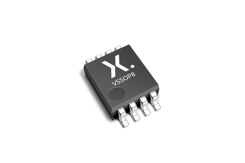
| 74AUP2G241DC | 0.8 - 3.6 | CMOS | ± 1.9 | 70 | 2 | ultra low | -40~125 | 203 | 30.4 | 113 | VSSOP8 |
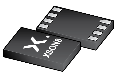
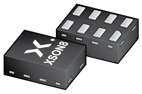
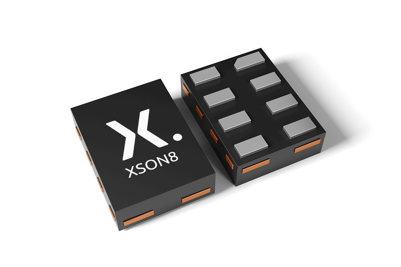
| 74AUP2G241GN | 0.8 - 3.6 | CMOS | ± 1.9 | 70 | 2 | ultra low | -40~125 | 238 | 148 | XSON8 | |
| 74AUP2G241GS | 0.8 - 3.6 | CMOS | ± 1.9 | 70 | 2 | ultra low | -40~125 | 276 | 146 | XSON8 | |
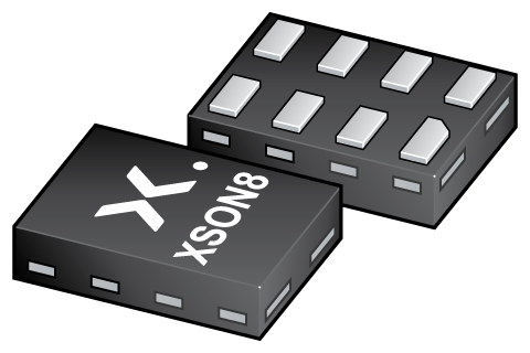
| 74AUP2G241GT | 0.8 - 3.6 | CMOS | ± 1.9 | 70 | 2 | ultra low | -40~125 | 327 | 5 | 157 | XSON8 |
封装
| 型号 | 可订购的器件编号,(订购码(12NC)) | 状态 | 标示 | 封装 | 外形图 | 回流焊/波峰焊 | 包装 |
|---|---|---|---|---|---|---|---|
| 74AUP2G241DC | 74AUP2G241DC,125 (935280738125) |
Active | p41 |
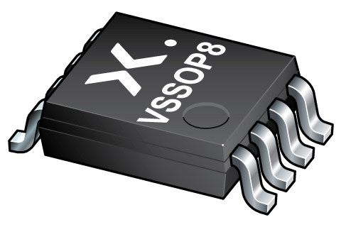
VSSOP8 (SOT765-1) |
SOT765-1 | SOT765-1_125 | |
| 74AUP2G241GN | 74AUP2G241GN,115 (935292225115) |
Active | p1 |
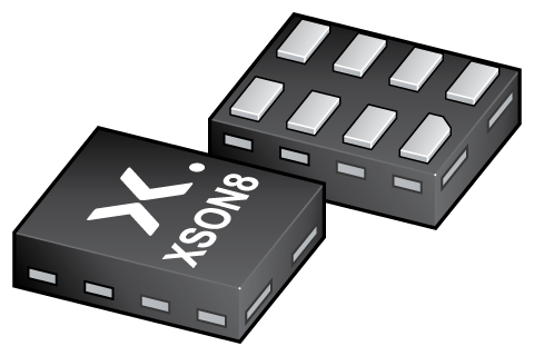
XSON8 (SOT1116) |
SOT1116 | SOT1116_115 | |
| 74AUP2G241GS | 74AUP2G241GS,115 (935292785115) |
Active | p1 |
XSON8 (SOT1203) |
SOT1203 | SOT1203_115 | |
| 74AUP2G241GT | 74AUP2G241GT,115 (935280739115) |
Active | p41 |
XSON8 (SOT833-1) |
SOT833-1 | SOT833-1_115 |
下表中的所有产品型号均已停产 。
| 型号 | 可订购的器件编号,(订购码(12NC)) | 状态 | 标示 | 封装 | 外形图 | 回流焊/波峰焊 | 包装 |
|---|---|---|---|---|---|---|---|
| 74AUP2G241GD | 74AUP2G241GD,125 (935288278125) |
Withdrawn / End-of-life | p41 |
XSON8 (SOT996-2) |
SOT996-2 | SOT996-2_125 | |
| 74AUP2G241GF | 74AUP2G241GF,115 (935291481115) |
Obsolete | p1 |
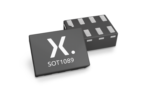
XSON8 (SOT1089) |
SOT1089 | SOT1089_115 | |
| 74AUP2G241GM | 74AUP2G241GM,125 (935281438125) |
Obsolete | p41 |
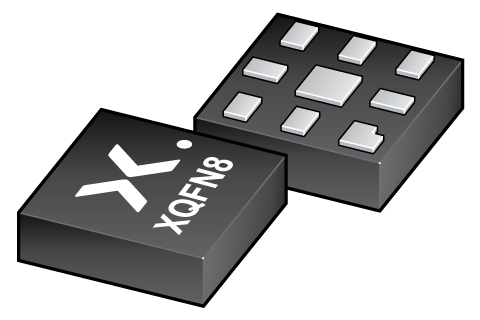
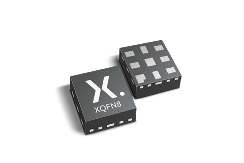
XQFN8 (SOT902-2) |
SOT902-2 | SOT902-2_125 |
环境信息
| 型号 | 可订购的器件编号 | 化学成分 | RoHS | RHF指示符 |
|---|---|---|---|---|
| 74AUP2G241DC | 74AUP2G241DC,125 | 74AUP2G241DC |
|
|
| 74AUP2G241GN | 74AUP2G241GN,115 | 74AUP2G241GN |
|
|
| 74AUP2G241GS | 74AUP2G241GS,115 | 74AUP2G241GS |
|
|
| 74AUP2G241GT | 74AUP2G241GT,115 | 74AUP2G241GT |
|
|
下表中的所有产品型号均已停产 。
| 型号 | 可订购的器件编号 | 化学成分 | RoHS | RHF指示符 |
|---|---|---|---|---|
| 74AUP2G241GD | 74AUP2G241GD,125 | 74AUP2G241GD |
|
|
| 74AUP2G241GF | 74AUP2G241GF,115 | 74AUP2G241GF |
|
|
| 74AUP2G241GM | 74AUP2G241GM,125 | 74AUP2G241GM |
|
|
文档 (31)
| 文件名称 | 标题 | 类型 | 日期 |
|---|---|---|---|
| 74AUP2G241 | Low-power dual buffer/line driver; 3-state | Data sheet | 2023-07-27 |
| AN10161 | PicoGate Logic footprints | Application note | 2002-10-29 |
| AN11052 | Pin FMEA for AUP family | Application note | 2019-01-09 |
| AN90063 | Questions about package outline drawings | Application note | 2025-10-22 |
| 001aah730 | Block diagram: 74AUP2G241DC, 74AUP2G241GD, 74AUP2G241GM, 74AUP2G241GT | Block diagram | 2009-11-03 |
| Nexperia_document_guide_MiniLogic_PicoGate_201901 | PicoGate leaded logic portfolio guide | Brochure | 2019-01-07 |
| Nexperia_document_guide_MiniLogic_MicroPak_201808 | MicroPak leadless logic portfolio guide | Brochure | 2018-09-03 |
| SOT765-1 | 3D model for products with SOT765-1 package | Design support | 2020-01-22 |
| SOT1089 | 3D model for products with SOT1089 package | Design support | 2019-10-07 |
| SOT1116 | 3D model for products with SOT1116 package | Design support | 2023-02-02 |
| SOT1203 | 3D model for products with SOT1203 package | Design support | 2023-02-02 |
| SOT833-1 | 3D model for products with SOT833-1 package | Design support | 2021-01-28 |
| aup2g241 | aup2g241 IBIS model | IBIS model | 2013-04-07 |
| Nexperia_document_leaflet_Logic_AUP_technology_portfolio_201904 | Nexperia_document_leaflet_Logic_AUP_technology_portfolio_201904 | Leaflet | 2019-04-12 |
| Nexperia_package_poster | Nexperia package poster | Leaflet | 2020-05-15 |
| VSSOP8_SOT765-1_mk | plastic, very thin shrink small outline package; 8 leads; 0.5 mm pitch; 2 mm x 2.3 mm x 1 mm body | Marcom graphics | 2017-01-28 |
| XSON8_SOT1089_mk | plastic, extremely thin small outline package; no leads; 8 terminals; 0.55 mm pitch; 1.35 mm x 1 mm x 0.5 mm body | Marcom graphics | 2017-01-28 |
| XQFN8_SOT902-2_mk | plastic, extremely thin quad flat package; 8 terminals; 0.55 mm pitch; 1.6 mm x 1.6 mm x 0.5 mm body | Marcom graphics | 2017-01-28 |
| XSON8_SOT1203_mk | plastic, leadless extremely thin small outline package; 8 terminals; 0.35 mm pitch; 1.35 mm x 1 mm x 0.35 mm body | Marcom graphics | 2019-02-04 |
| REFLOW_BG-BD-1 | Reflow soldering profile | Other type | 2026-02-10 |
| SOT765-1 | plastic, very thin shrink small outline package; 8 leads; 0.5 mm pitch; 2 mm x 2.3 mm x 1 mm body | Package information | 2022-06-03 |
| SOT996-2 | plastic, leadless extremely thin small outline package; 8 terminals; 0.5 mm pitch; 3 mm x 2 mm x 0.5 mm body | Package information | 2020-04-21 |
| SOT1089 | plastic, leadless extremely thin small outline package; 8 terminals; 0.35 mm pitch; 1.35 mm x 1 mm x 0.5 mm body | Package information | 2022-06-03 |
| SOT902-2 | plastic, leadless extremely thin quad flat package; 8 terminals; 0.5 mm pitch; 1.6 mm x 1.6 mm x 0.5 mm body | Package information | 2020-04-21 |
| SOT1116 | plastic, leadless extremely thin small outline package; 8 terminals; 0.3 mm pitch; 1.2 mm x 1 mm x 0.35 mm body | Package information | 2022-06-02 |
| SOT1203 | plastic, leadless extremely thin small outline package; 8 terminals; 0.35 mm pitch; 1.35 mm x 1 mm x 0.35 mm body | Package information | 2022-06-03 |
| SOT833-1 | plastic, leadless extremely thin small outline package; 8 terminals; 0.5 mm pitch; 1 mm x 1.95 mm x 0.5 mm body | Package information | 2022-06-03 |
| MAR_SOT1089 | MAR_SOT1089 Topmark | Top marking | 2013-06-03 |
| MAR_SOT1116 | MAR_SOT1116 Topmark | Top marking | 2013-06-03 |
| MAR_SOT1203 | MAR_SOT1203 Topmark | Top marking | 2013-06-03 |
| MAR_SOT833 | MAR_SOT833 Topmark | Top marking | 2013-06-03 |
支持
如果您需要设计/技术支持,请告知我们并填写 应答表 我们会尽快回复您。
模型
| 文件名称 | 标题 | 类型 | 日期 |
|---|---|---|---|
| SOT765-1 | 3D model for products with SOT765-1 package | Design support | 2020-01-22 |
| SOT1089 | 3D model for products with SOT1089 package | Design support | 2019-10-07 |
| SOT1116 | 3D model for products with SOT1116 package | Design support | 2023-02-02 |
| SOT1203 | 3D model for products with SOT1203 package | Design support | 2023-02-02 |
| SOT833-1 | 3D model for products with SOT833-1 package | Design support | 2021-01-28 |
| aup2g241 | aup2g241 IBIS model | IBIS model | 2013-04-07 |
Ordering, pricing & availability
样品
作为 Nexperia 的客户,您可以通过我们的销售机构订购样品。
如果您没有 Nexperia 的直接账户,我们的全球和地区分销商网络可为您提供 Nexperia 样品支持。查看官方经销商列表。