


74LV1T34-Q100
Single supply translating buffer
The 74LV1T34-Q100 is a single, level translating buffer. The low threshold inputs support 1.8 V input logic at VCC = 3.3 V and can be used in 1.8 V to 3.3 V level up translation. In addition, the 5 V tolerant input pins enable level down translation (3.3 V to 2.5 V output at VCC = 2.5 V). The output level is referenced to the supply voltage and supports 1.8 V, 2.5 V, 3.3 V and 5.0 V CMOS levels. The wide VCC range permits the generation of output levels to connect to controllers or processors.
This product has been qualified to the Automotive Electronics Council (AEC) standard Q100 (Grade 1) and is suitable for use in automotive applications.
Features and benefits
Automotive product qualification in accordance with AEC-Q100 (Grade 1)
Specified from -40 °C to +85 °C and from -40 °C to +125 °C
Single supply voltage translator at 1.8 V, 2.5 V, 3.3 V and 5.0 V
Up translation
1.2 V to 1.8 V at VCC = 1.8 V
1.5 V to 2.5 V at VCC = 2.5 V
1.8 V to 3.3 V at VCC = 3.3 V
3.3 V to 5.0 V at VCC = 5.0 V
Down translation
3.3 V to 1.8 V at VCC = 1.8 V
3.3 V to 2.5 V at VCC = 2.5 V
5.0 V to 3.3 V at VCC = 3.3 V
5 V tolerant inputs
Latch-up performance exceeds 250 mA per JESD 78 Class II
ESD protection:
HBM: ANSI/ESDA/JEDEC JS-001 class 2 exceeds 2000 V
CDM: ANSI/ESDA/JEDEC JS-002 class C3 exceeds 1000 V
Applications
Portable applications
PC and notebooks
Industrial controller
Telecom
参数类型
| 型号 | VCC (V) | Logic switching levels | Output drive capability (mA) | Nr of bits | Power dissipation considerations | Tamb (°C) | Rth(j-a) (K/W) | Ψth(j-top) (K/W) | Rth(j-c) (K/W) | Package name |
|---|---|---|---|---|---|---|---|---|---|---|
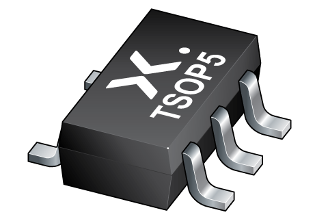
| 74LV1T34GV-Q100 | 1.6 - 5.5 | CMOS | ± 8 | 1 | low | -40~125 | 276 | 66.9 | 173 | TSOP5 |
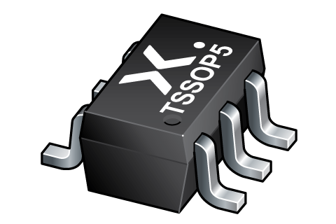
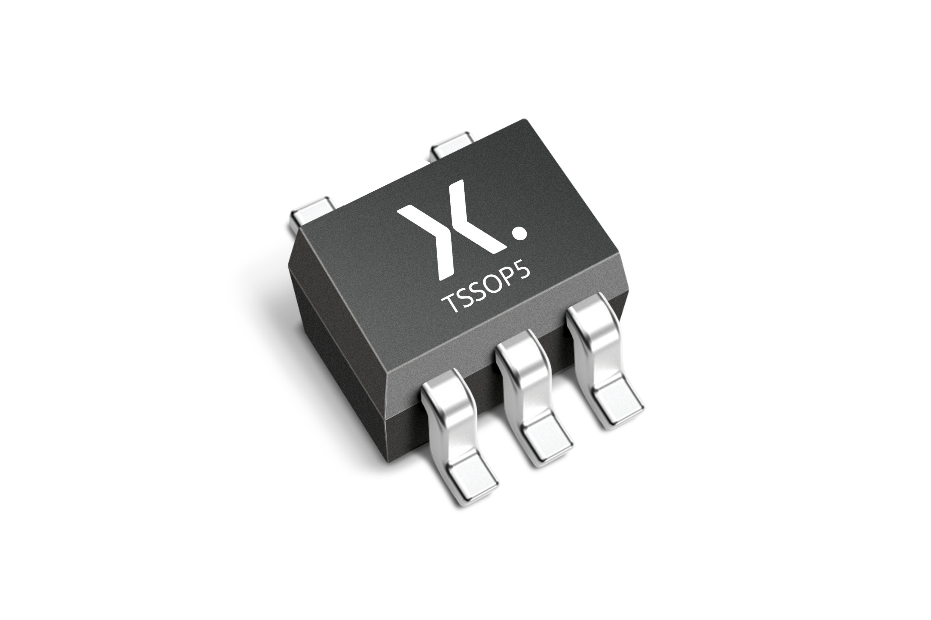
| 74LV1T34GW-Q100 | 1.6 - 5.5 | CMOS | ± 8 | 1 | low | -40~125 | 316 | 85.8 | 186 | TSSOP5 |
封装
| 型号 | 可订购的器件编号,(订购码(12NC)) | 状态 | 标示 | 封装 | 外形图 | 回流焊/波峰焊 | 包装 |
|---|---|---|---|---|---|---|---|
| 74LV1T34GV-Q100 | 74LV1T34GV‑Q100H (935691086125) |
Active | SQ |
TSOP5 (SOT753) |
SOT753 |
WAVE_BG-BD-1
|
SOT753_125 |
| 74LV1T34GW-Q100 | 74LV1T34GW‑Q100H (935691281125) |
Active | SQ |
TSSOP5 (SOT353-1) |
SOT353-1 |
WAVE_BG-BD-1
|
SOT353-1_125 |
环境信息
| 型号 | 可订购的器件编号 | 化学成分 | RoHS | RHF指示符 |
|---|---|---|---|---|
| 74LV1T34GV-Q100 | 74LV1T34GV‑Q100H | 74LV1T34GV-Q100 |
|
|
| 74LV1T34GW-Q100 | 74LV1T34GW‑Q100H | 74LV1T34GW-Q100 |
|
|
文档 (13)
| 文件名称 | 标题 | 类型 | 日期 |
|---|---|---|---|
| 74LV1T34_Q100 | Single supply translating buffer | Data sheet | 2023-12-06 |
| AN90063 | Questions about package outline drawings | Application note | 2025-10-22 |
| Nexperia_document_guide_MiniLogic_PicoGate_201901 | PicoGate leaded logic portfolio guide | Brochure | 2019-01-07 |
| SOT753 | 3D model for products with SOT753 package | Design support | 2019-01-22 |
| SOT353-1 | 3D model for products with SOT353-1 package | Design support | 2019-09-23 |
| lv1t34 | IBIS model of 74LV1T34 | IBIS model | 2018-01-19 |
| Nexperia_package_poster | Nexperia package poster | Leaflet | 2020-05-15 |
| TSSOP5_SOT353-1_mk | plastic, thin shrink small outline package; 5 leads; 0.65 mm pitch; 2 mm x 1.25 mm x 0.95 mm body | Marcom graphics | 2018-07-25 |
| REFLOW_BG-BD-1 | Reflow soldering profile | Other type | 2026-02-10 |
| SOT753 | plastic, surface-mounted package; 5 leads; 0.95 mm pitch; 2.9 mm x 1.5 mm x 1 mm body | Package information | 2022-05-31 |
| SOT353-1 | plastic thin shrink small outline package; 5 leads; body width 1.25 mm | Package information | 2022-11-15 |
| MAR_SOT753 | MAR_SOT753 Topmark | Top marking | 2013-06-03 |
| WAVE_BG-BD-1 | Wave soldering profile | Wave soldering | 2021-09-08 |
支持
如果您需要设计/技术支持,请告知我们并填写 应答表 我们会尽快回复您。
Ordering, pricing & availability
样品
作为 Nexperia 的客户,您可以通过我们的销售机构订购样品。
如果您没有 Nexperia 的直接账户,我们的全球和地区分销商网络可为您提供 Nexperia 样品支持。查看官方经销商列表。