双极性晶体管

二极管

ESD保护、TVS、滤波和信号调节ESD保护

MOSFET

氮化镓场效应晶体管(GaN FET)

绝缘栅双极晶体管(IGBTs)

模拟和逻辑IC

汽车应用认证产品(AEC-Q100/Q101)

NCA6416BY

The NCA6416-Q100 is a versatile 16-bit general-purpose I‌‌/‌‌O expander designed for microcontrollers that need additional I/O pins. It communicates via an I²C-bus interface, making it ideal for applications with minimal space and wiring, such as battery-powered devices using sensors, keypads, push buttons or LED control for managing LED brightness.

Nexperia's I/O expanders feature a dual power supply architecture with two inputs: VCCI and VCCP. This design enables seamless level translation, supporting mixed-voltage environments. VCCI powers the I²C interface and must be connected to the same voltage as the host microcontroller's I²C bus (SDA/SCL), which can range from 1.65 V to 5.5 V. VCCP powers the internal core and the I/O pins on Port P, defining the voltage level for the connected peripherals. This allows a low-voltage microcontroller to interface with higher-voltage peripherals without additional external circuitry.

The NCA6416-Q100 contains four pairs of 8-bit registers: Configuration, Input, Output, and Polarity Inversion. By default, all I/O pins are configured as inputs at power-on. A system controller can dynamically reconfigure these pins as inputs or outputs by writing to the Configuration register. The Input and Output registers store the current state of each pin. The Polarity Inversion register allows to invert the polarity of the input pins, which can simplify logic in system by eliminating the need for external gates.

The device has an open-drain INT output that triggers when an input pin changes state. This interrupt can be connected to a microcontroller's interrupt pin, allowing the NCA6416-Q100 to notify the host of a change without the need for constant polling over the I²C bus. This feature makes the NCA6416-Q100 an efficient and passive I²C target device.

To recover from errors like I²C time-outs, a system controller can drive the RESET input low. This resets all registers to their default state and reinitializes the I²C/SMBus interface without requiring a power cycle.

A hardware ADDR pin allows to program the device's I²C address, making it possible to use up to two NCA6416-Q100 devices on a single bus.

In addition, each output pin on Port P can sink up to 25 mA, making it suitable for directly driving low-current loads like LEDs.

Features and benefits

  • I²C-bus to parallel port expander

  • Supply voltage range of 1.65 V to 5.5 V

  • Allows bidirectional voltage-level translation and GPIO expansion between:

    • 1.8 V SCL/SDA and 1.8 V, 2.5 V, 3.3 V or 5 V Port P

    • 2.5 V SCL/SDA and 1.8 V, 2.5 V, 3.3 V or 5 V Port P

    • 3.3 V SCL/SDA and 1.8 V, 2.5 V, 3.3 V or 5 V Port P

    • 5 V SCL/SDA and 1.8 V, 2.5 V, 3.3 V or 5 V Port P

  • Low standby current consumption:

    • 1.5 μA typical at 5 V VCC

    • 1.0 μA typical at 3.3 V VCC

  • Schmitt-trigger action allows slow input transition and better switching noise immunity at the SCL and SDA inputs

    • Vhys = 0.18 V (typical) at 1.8 V

    • Vhys = 0.25 V (typical) at 2.5 V

    • Vhys = 0.33 V (typical) at 3.3 V

    • Vhys = 0.5 V (typical) at 5 V

  • 5 V tolerant I/O ports

  • Active LOW reset input (RESET)

  • Open-drain active LOW interrupt output (INT)

  • 400 kHz Fast-mode I²C-bus

  • Input/Output Configuration register

  • Polarity Inversion register

  • Internal power-on reset

  • Glitch free power-up

  • No power up sequence required

  • Partial power down supported

  • Noise filter on SCL/SDA inputs

  • Latched outputs with 25 mA drive maximum capability for directly driving LEDs

  • Latch-up performance exceeds 100 mA per JESD 78, Class II

  • ESD protection:

    • HBM: ANSI/ESDA/JEDEC JS-001 class 2 exceeds 2000 V

    • CDM: ANSI/ESDA/JEDEC JS-002 class C3 exceeds 1000 V

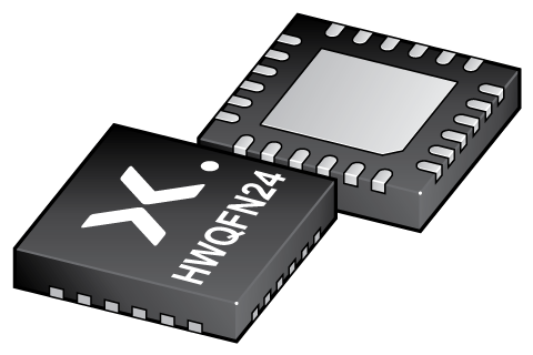
  • Packages offered: TSSOP24, HWQFN24

  • Specified from -40 °C to +85 °C and from -40 °C to +125 °C

参数类型

型号 Package name
NCA6416BY HWQFN24

封装

型号 可订购的器件编号,(订购码(12NC)) 状态 标示 封装 外形图 回流焊/波峰焊 包装
NCA6416BY NCA6416BYHP
(935691813128)
Development CA6416 SOT8041-1
HWQFN24
(SOT8041-1)
SOT8041-1 SOT8041-1_128

环境信息

型号 可订购的器件编号 化学成分 RoHS RHF指示符
NCA6416BY NCA6416BYHP NCA6416BY rohs rhf rhf
品质及可靠性免责声明

文档 (5)

文件名称 标题 类型 日期
NCA6416 Low-voltage translating 16-bit I²C-bus/SMBus I/O expander Data sheet 2025-08-20
AN90063 Questions about package outline drawings Application note 2025-06-13
nca6416 NCA6416 IBIS model IBIS model 2025-08-30
SOT8041-1 plastic thermal enhanced very very thin Quad Flat packages, no leads;24 terminals; 0.5 mm pitch; 4 x 4 x 0.75 mm body Package information 2024-04-23
SOT8041-1_128 QFN4x4 24L; Reel pack for SMD, 13"; Q2/T3 product orientation Packing information 2022-08-01

支持

如果您需要设计/技术支持,请告知我们并填写 应答表 我们会尽快回复您。


Longevity

The Nexperia Longevity Program is aimed to provide our customers information from time to time about the expected time that our products can be ordered. The NLP is reviewed and updated regularly by our Executive Management Team. View our longevity program here.


模型

文件名称 标题 类型 日期
nca6416 NCA6416 IBIS model IBIS model 2025-08-30

订购、定价与供货

型号 Orderable part number Ordering code (12NC) 状态 包装 Packing Quantity 在线购买

样品

作为 Nexperia 的客户,您可以通过我们的销售机构订购样品。

如果您没有 Nexperia 的直接账户,我们的全球和地区分销商网络可为您提供 Nexperia 样品支持。查看官方经销商列表

How does it work?

The interactive datasheets are based on the Nexperia MOSFET precision electrothermal models. With our interactive datasheets you can simply specify your own conditions interactively. Start by changing the values of the conditions. You can do this by using the sliders in the condition fields. By dragging the sliders you will see how the MOSFET will perform at the new conditions set.

可订购部件

型号 可订购的器件编号 订购代码(12NC) 封装 从经销商处购买
NCA6416BY NCA6416BYHP 935691813128 SOT8041-1 订单产品