


74AVC4T3144
4-bit dual-supply buffer/level translator; 3-state
The 74AVC4T3144 is a 4-bit, dual-supply level translating buffer with 3-state outputs. It features four data inputs (An and B4), four data outputs (YBn and YA4), and an output enable input (OE). The device is configured to translate three inputs from VCC(A) to VCC(B) and one input from VCC(B) to VCC(A). OE, An and YA4 are referenced to VCC(A) and YBn and B4 are referenced to VCC(B). A HIGH on OE causes the outputs to assume a high-impedance OFF-state.
The device is fully specified for partial power-down applications using IOFF. The IOFF circuitry disables outputs, preventing any damaging backflow current through the device when it is powered down. In suspend mode when either VCC(A) or VCC(B) are at GND level, all outputs are in the high-impedance OFF-state.
Features and benefits
Wide supply voltage range:
VCC(A): 0.8 V to 3.6 V
VCC(B): 0.8 V to 3.6 V
Complies with JEDEC standards:
JESD8-12 (0.8 V to 1.3 V)
JESD8-11 (0.9 V to 1.65 V)
JESD8-7 (1.2 V to 1.95 V)
JESD8-5 (1.8 V to 2.7 V)
JESD8-B (2.7 V to 3.6 V)
Maximum data rates:
380 Mbit/s (≥ 1.8 V to 3.3 V translation)
200 Mbit/s (≥ 1.1 V to 3.3 V translation)
200 Mbit/s (≥ 1.1 V to 2.5 V translation)
200 Mbit/s (≥ 1.1 V to 1.8 V translation)
150 Mbit/s (≥ 1.1 V to 1.5 V translation)
100 Mbit/s (≥ 1.1 V to 1.2 V translation)
Suspend mode
Latch-up performance exceeds 100 mA per JESD 78 Class II
Inputs accept voltages up to 3.6 V
IOFF circuitry provides partial Power-down mode operation
ESD protection:
HBM: ANSI/ESDA/JEDEC JS-001 class 3B exceeds 8000 V
CDM: ANSI/ESDA/JEDEC JS-002 class C3 exceeds 1000 V
Specified from -40 °C to +85 °C and -40 °C to +125 °C
参数类型
| 型号 | VCC (V) | Logic switching levels | Output drive capability (mA) | fmax (MHz) | Nr of bits | Power dissipation considerations | Tamb (°C) | Rth(j-a) (K/W) | Ψth(j-top) (K/W) | Rth(j-c) (K/W) | Package name |
|---|---|---|---|---|---|---|---|---|---|---|---|
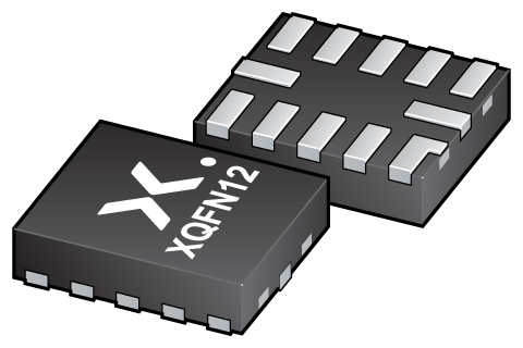
| 74AVC4T3144GU12 | n.a. | CMOS/LVTTL | ± 12 | 190 | 4 | very low | -40~125 | 188 | 6.2 | 95.8 | XQFN12 |
| 74AVC4T3144GU12-Q100 | n.a. | CMOS/LVTTL | ± 12 | 190 | 4 | very low | -40~125 | 188 | 6.2 | 95.8 | XQFN12 |
封装
| 型号 | 可订购的器件编号,(订购码(12NC)) | 状态 | 标示 | 封装 | 外形图 | 回流焊/波峰焊 | 包装 |
|---|---|---|---|---|---|---|---|
| 74AVC4T3144GU12 | 74AVC4T3144GU12X (935690174115) |
Active | Bd |

XQFN12 (SOT1174-1) |
SOT1174-1 | SOT1174-1_115 | |
| 74AVC4T3144GU12-Q100 | 74AVC4T3144GU12‑QX (935690912115) |
Active | Bd |
XQFN12 (SOT1174-1) |
SOT1174-1 | SOT1174-1_115 |
环境信息
| 型号 | 可订购的器件编号 | 化学成分 | RoHS | RHF指示符 |
|---|---|---|---|---|
| 74AVC4T3144GU12 | 74AVC4T3144GU12X | 74AVC4T3144GU12 |
|
|
| 74AVC4T3144GU12-Q100 | 74AVC4T3144GU12‑QX | 74AVC4T3144GU12-Q100 |
|
|
文档 (8)
| 文件名称 | 标题 | 类型 | 日期 |
|---|---|---|---|
| 74AVC4T3144 | 4-bit dual-supply buffer/level translator; 3-state | Data sheet | 2024-07-02 |
| AN90007 | Pin FMEA for AVC family | Application note | 2018-11-30 |
| AN90063 | Questions about package outline drawings | Application note | 2026-06-17 |
| SOT1174-1 | 3D model for products with SOT1174-1 package | Design support | 2021-01-28 |
| avc4t3144 | IBIS model of 74AVC4T3144 | IBIS model | 2017-12-22 |
| 74AVC4T3144_and_74LVC4T3144_leaflet | Dual supply translating buffers/line drivers | Leaflet | 2018-03-09 |
| Nexperia_package_poster | Nexperia package poster | Leaflet | 2020-05-15 |
| SOT1174-1 | plastic, leadless extremely thin quad flat package; 12 terminals; 0.4 mm pitch; 2 mm x 1.7 mm x 0.5 mm body | Package information | 2024-04-11 |
支持
如果您需要设计/技术支持,请告知我们并填写 应答表 我们会尽快回复您。
Ordering, pricing & availability
样品
作为 Nexperia 的客户,您可以通过我们的销售机构订购样品。
如果您没有 Nexperia 的直接账户,我们的全球和地区分销商网络可为您提供 Nexperia 样品支持。查看官方经销商列表。