NGD4300-Q100
4 A peak high-performance dual MOSFET gate driver
The NGD4300-Q100 is a high-performance gate driver designed to drive both high-side and low-side N-channel MOSFETs in a synchronous buck or a half-bridge configuration. The floating high-side driver can work with rail voltages up to 120 V and uses a bootstrap supply with an integrated diode. Both low-side and high-side output drivers have an independent undervoltage lockout (UVLO) circuit which disables the output driver when the driver supply is below its threshold level. The NGD4300-Q100 accepts input control signals complying with both TTL and CMOS signaling as low as 2.5 V (±10%). The low voltage, provided by an internal voltage regulator, is used to supply circuitry in signal paths controlling the low-side and high-side power switches. This enables a low-power operation and a better controlled driver performance irrespective of the IC supply voltage.
Excellent delay matching of 1 ns typical is achieved for the low-side and high-side signal paths. The 4 A peak source and sink current capability of the driver’s output stage guarantees short rise- and fall-times even at high loads.
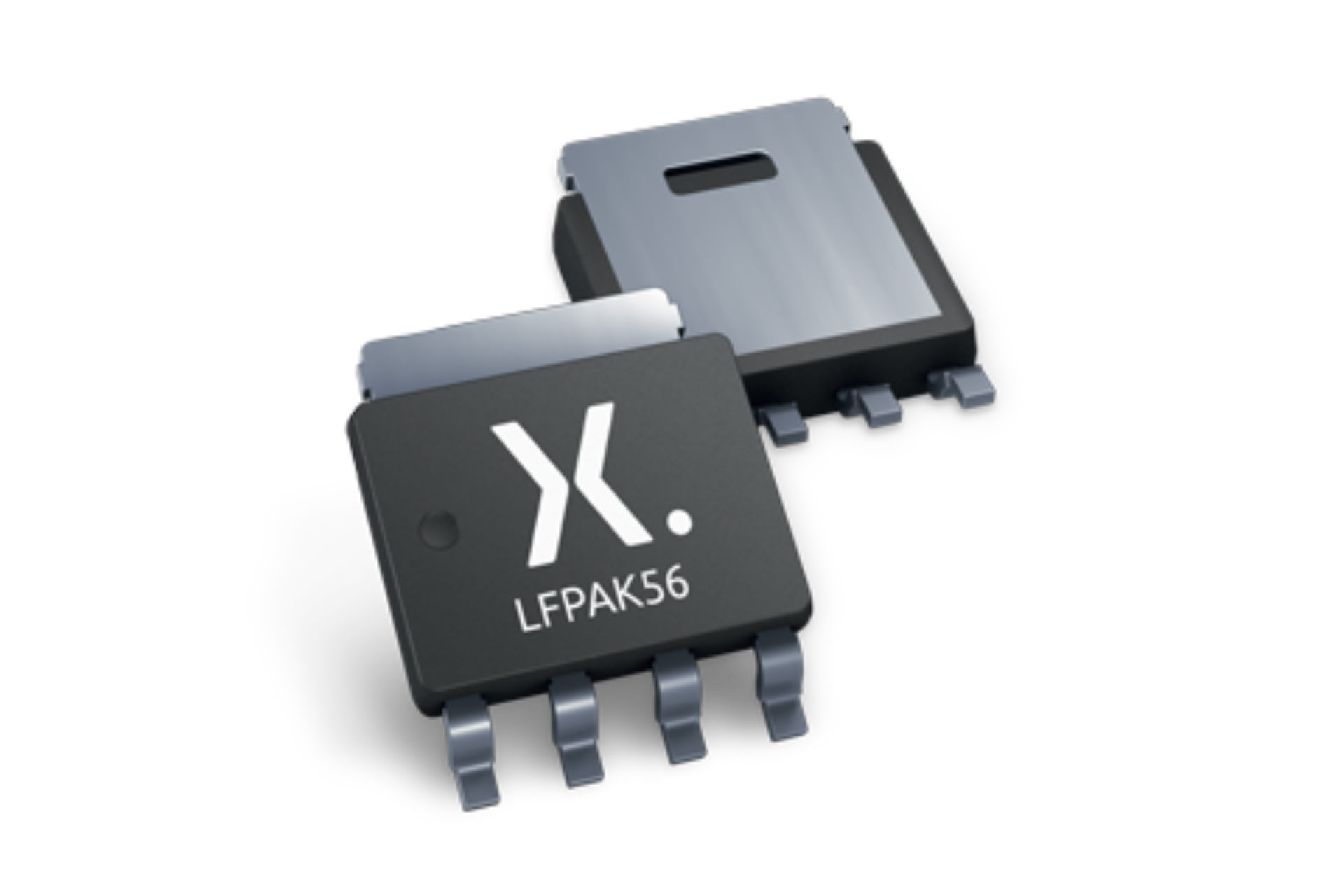
The NGD4300-Q100 is offered in the HSO8 package, and operates over an extended −40 °C to +125 °C temperature range.
This product has been qualified to the Automotive Electronics Council (AEC) standard Q100 (Grade 1) and is suitable for use in automotive applications.
 |
Features and benefits
- Automotive product qualification in accordance with AEC-Q100 (Grade 1)
- Specified from -40 °C to +125 °C
- Input signals complying with both TTL and CMOS signaling of 2.5 V, 3.3 V, and 5 V
- Output signals with 1 ns propagation delay matching (typical)
- Propagation times of 13 ns (typical)
- Switching frequency up to 1 MHz
- 4 A peak source and 5 A sink current capability of the gate driver output stage
- 4 ns rise and 3.5 ns fall times with 1000 pF loads
- Bootstrap supply voltage up to 120 V using an integrated bootstrap diode
- 8 V to 17 V VDD operation range
- Undervoltage protection for both low-side and high-side supplies
- Low-power consumption (IDDO) of 0.6 mA (typical)
- 8 pin HSO8 package
- ESD protection:
HBM: ANSI/ESDA/JEDEC JS-001 class 2 exceeds 2000 V
CDM: ANSI/ESDA/JEDEC JS-002 class C3 exceeds 1000 V
Applications
Current-fed, push-pull converters
Two-switch forward power converters
Class-D audio amplifiers
Solid-state motor drives
封装
| 型号 | 可订购的器件编号,(订购码(12NC)) | 状态 | 标示 | 封装 | 外形图 | 回流焊/波峰焊 | 包装 |
|---|---|---|---|---|---|---|---|
| NGD4300DD-Q100 | NGD4300DD‑Q100J (935691643118) |
Active | NGD4300 |

HSO8 (SOT8063-1) |
SOT8063-1 | SOT8063-1_118 |
文档 (3)
| 文件名称 | 标题 | 类型 | 日期 |
|---|---|---|---|
| NGD4300_Q100 | 4 A peak high-performance dual MOSFET gate driver | Data sheet | 2025-07-21 |
| AN90063 | Questions about package outline drawings | Application note | 2025-10-22 |
| SOT8063-1 | plastic thermal enhanced small outline package; 8 leads; 1.27 mm pitch;4.9 mm × 3.9 mm ×1.7 mm body; exposed die pad | Package information | 2024-09-24 |
支持
如果您需要设计/技术支持,请告知我们并填写 应答表 我们会尽快回复您。
模型
No documents available
Ordering, pricing & availability
样品
作为 Nexperia 的客户,您可以通过我们的销售机构订购样品。
如果您没有 Nexperia 的直接账户,我们的全球和地区分销商网络可为您提供 Nexperia 样品支持。查看官方经销商列表。
