


- 产品细节
- 文档
- 支持
- 交互式数据手册
产品细节
Features and benefits
Wide supply voltage range from 1.2 V to 3.6 V
CMOS low-power consumption
Direct interface with TTL levels
Current drive ± 24 mA at 3.0 V
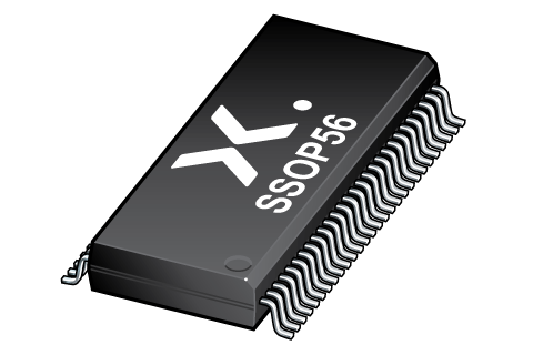
MULTIBYTE™ flow-through standard pin-out architecture
Low inductance multiple VCC and GND pins for minimum noise and ground bounce
Output drive capability 50 Ω transmission lines at 85°C
All data inputs have bushold
Complies with JEDEC standard no. 8-1A
Complies with JEDEC standards:
JESD8-5 (2.3 V to 2.7 V)
JESD8B/JESD36 (2.7 V to 3.6 V)
ESD protection:
- HBM: ANSI/ESDA/JEDEC JS-001 class 2 exceeds 2000 V
- CDM: ANSI/ESDA/JEDEC JS-002 class C3 exceeds 1000 V
- Specified from -40 °C to +85 °C
Register once, drag and drop ECAD models into your CAD tool and speed up your design.
More information品质及可靠性免责声明
支持
如果您有支持方面的疑问,请告知我们。如需获得设计支持,请告知我们并填写技术支持表格,我们会尽快回复您。
请访问我们的社区论坛或联系我们。
Longevity
The Nexperia Longevity Program is aimed to provide our customers information from time to time about the expected time that our products can be ordered. The NLP is reviewed and updated regularly by our Executive Management Team. View our longevity program here.
交互式数据手册
How does it work?
The interactive data sheets are based on the Nexperia MOSFET precision electrothermal models. With our interactive data sheets you can simply specify your own conditions interactively. Start by changing the values of the conditions. You can do this by using the sliders in the condition fields. By dragging the sliders you will see how the MOSFET will perform at the new conditions set.
交互式数据手册