
特性
-
Wide operating range: 1.5 V to 5.5 V
-
2x SP4T-Z functionality
-
Rail-to-Rail operation on analog signal pins
-
Injection current control
-
1.8 V digital logic thresholds
-
Digital pins compatible with 1.8 V logic thresholds across full VCC range
-
Removes need for up-translation device for compatibility with low voltage GPIOs
-
-
Ioff circuitry
-
Enables wider latitude for power sequencing considerations
-
Isolates backflow between supply rail and any biased digital/analog input when VCC = 0 V
-
Prevents any biased digital/analog input from backpowering VCC when VCC = 0 V
-
Maintains Hi-Z state of analog switch when VCC = 0 V
-
-
5.5 V overvoltage tolerant digital inputs
-
Supports switching of 5.5 V digital signals across full VCC operating range
-
Removes need for down-translation when switching thresholds are met
-
-
Pin compatible with industry standard 4052 and 4852 analog switch products
-
ESD protection:
-
HBM: ANSI/ESDA/JEDEC JS-001 class 2 exceeds 2000 V
-
CDM: ANSI/ESDA/JEDEC JS-002 class C2b exceeds 750 V
-
-
Specified from -40 °C to +85 °C and from -40 °C to +125 °C
目标应用
-
Analog or digital multiplexing/demultiplexing
-
System monitoring and diagnostics
-
Enterprise computing
-
Appliances
参数类型
| Type number | Product status | Configuration | VCC (V) | Logic switching levels | RON (Ω) | RON(FLAT) (Ω) | f(-3dB) (MHz) | THD (%) | Xtalk (dB) | Power dissipation considerations | Tamb (°C) | Rth(j-a) (K/W) | Ψth(j-top) (K/W) | Rth(j-c) (K/W) | Package name |
|---|---|---|---|---|---|---|---|---|---|---|---|---|---|---|---|
| NMUX1309BQ | Production | SP4T-Z | 1.5 - 5.5 | CMOS | 60 | - | 380 | - | -105 | very low | -40~125 | 93 | 62.0 | 13.8 | DHVQFN16 |
| NMUX1309PW | Production | SP4T-Z | 1.5 - 5.5 | CMOS | 60 | - | 380 | - | -105 | very low | -40~125 | 139 | 64.0 | 6.9 | TSSOP16 |
(-) dash denotes: "Parameter value not specified for this product"
封装
| 型号 | 封装 | 尺寸版本 | 回流焊/波峰焊 | 包装 | 状态 | 标示 | 可订购的器件编号,(订购码(12NC)) |
|---|---|---|---|---|---|---|---|
| NMUX1309BQ | 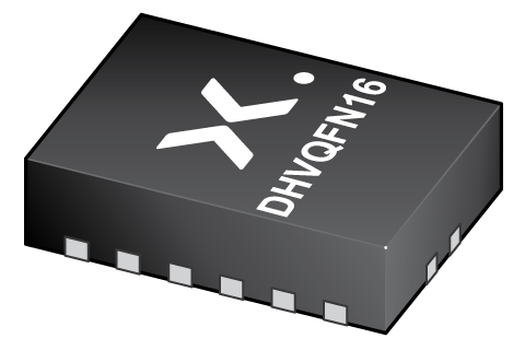 DHVQFN16 (SOT763-1) | SOT763-1 | SOT763-1_115 | Active | NM1309 | NMUX1309BQX ( 9356 914 15115 ) | |
| NMUX1309PW | 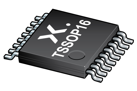 TSSOP16 (SOT403-1) | SOT403-1 | SSOP-TSSOP-VSO-WAVE | SOT403-1_118 | Active | NMU1309 | NMUX1309PWJ ( 9356 914 17118 ) |
环境信息
| 型号 | 可订购的器件编号 | 化学成分 | RoHS | RHF指示符 | 无铅转换日期 |
|---|---|---|---|---|---|
| NMUX1309BQ | NMUX1309BQX | NMUX1309BQ | |||
| NMUX1309PW | NMUX1309PWJ | NMUX1309PW |
文档 (7)
| 文件名称 | 标题 | 类型 | 日期 |
|---|---|---|---|
| NMUX1309 | 1.5 V to 5.5 V, dual 4-channel switch analog multiplexer and demultiplexer with injection-current control | Data sheet | 2024-04-16 |
| AN90051 | Pin FMEA for NMUX130x family | Application note | 2024-02-13 |
| 1_8V_General_purpose_injection_control_analog_switch_leaflet | 1.8 V General purpose SP8T-Z and 2x SP4T-Z analog switches with injection current control | Leaflet | 2024-03-05 |
| UM90026 | NMUX1308; NMUX1309 evaluation board | User manual | 2024-01-18 |
| SOT763-1 | plastic, leadless dual in-line compatible thermal enhanced very thin quad flat package; 16 terminals; 0.5 mm pitch; 3.5 mm x 2.5 mm x 1 mm body | Package information | 2023-05-11 |
| SOT403-1 | plastic, thin shrink small outline package; 16 leads; 5 mm x 4.4 mm x 1.2 mm body | Package information | 2023-11-08 |
| SSOP-TSSOP-VSO-WAVE | Footprint for wave soldering | Wave soldering | 2009-10-08 |
支持
如果您需要设计/技术支持,请告知我们并填写 应答表, 我们会尽快回复您。
订购、定价与供货
样品
安世半导体客户可通过我们的销售机构或直接通过在线样品商店订购样品: https://extranet.nexperia.com.
样品订单通常需要2-4天寄送时间。
如果您尚未取得安世半导体的直接采购帐号,我们的全球与区域经销网络可以协助您取得样品。