
特性
-
Automotive product qualification in accordance with AEC-Q100 (Grade 1)
-
Specified from -40 °C to +85 °C and from -40 °C to +125 °C
-
-
Wide supply voltage range from 1.0 V to 5.5 V
-
CMOS low power dissipation
-
Optimized for low voltage applications: 1.0 V to 3.6 V
-
Accepts TTL input levels between VCC = 2.7 V and VCC = 3.6 V
-
Typical output ground bounce < 0.8 V at VCC = 3.3 V and Tamb = 25 °C
-
Typical HIGH-level output voltage (VOH) undershoot: > 2 V at VCC = 3.3 V and Tamb = 25 °C
- Latch-up performance exceeds 100 mA per JESD 78 Class II Level B
- Complies with JEDEC standards:
- JESD8-7 (1.65 V to 1.95 V)
- JESD8-5 (2.3 V to 2.7 V)
- JESD8C (2.7 V to 3.6 V)
- JESD36 (4.5 V to 5.5 V)
-
ESD protection:
-
HBM: ANSI/ESDA/JEDEC JS-001 class 2 exceeds 2000 V
-
CDM: ANSI/ESDA/JEDEC JS-002 class C3 exceeds 1000 V
-
目标应用
-
Wave and pulse shapers for highly noisy environments
-
Astable multivibrators
-
Monostable multivibrators
参数类型
| Type number | Product status | VCC (V) | Logic switching levels | Output drive capability (mA) | fmax (MHz) | Nr of bits | Power dissipation considerations | Tamb (°C) | Rth(j-a) (K/W) | Rth(j-c) (K/W) | Package name |
|---|---|---|---|---|---|---|---|---|---|---|---|
| 74LV14D-Q100 | Production | 1.0 - 5.5 | TTL | ± 12 | 30 | 6 | low | -40~125 | 91 | 48 | SO14 |
| 74LV14PW-Q100 | Production | 1.0 - 5.5 | TTL | ± 12 | 30 | 6 | low | -40~125 | 129 | 54.1 | TSSOP14 |
封装
| 型号 | 封装 | 尺寸版本 | 回流焊/波峰焊 | 包装 | 状态 | 标示 | 可订购的器件编号,(订购码(12NC)) |
|---|---|---|---|---|---|---|---|
| 74LV14D-Q100 | 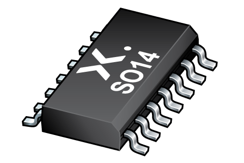 SO14 (SOT108-1) | SOT108-1 | SO-SOJ-REFLOW SO-SOJ-WAVE | SOT108-1_118 | Active | 74LV14D | 74LV14D-Q100J ( 9356 915 98118 ) |
| 74LV14PW-Q100 | 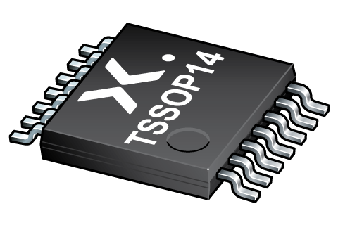 TSSOP14 (SOT402-1) | SOT402-1 | SSOP-TSSOP-VSO-WAVE | SOT402-1_118 | Active | LV14 | 74LV14PW-Q100J ( 9356 916 03118 ) |
环境信息
| 型号 | 可订购的器件编号 | 化学成分 | RoHS | RHF指示符 | 无铅转换日期 |
|---|---|---|---|---|---|
| 74LV14D-Q100 | 74LV14D-Q100J | 74LV14D-Q100 | |||
| 74LV14PW-Q100 | 74LV14PW-Q100J | 74LV14PW-Q100 |
文档 (7)
| 文件名称 | 标题 | 类型 | 日期 |
|---|---|---|---|
| 74LV14_Q100 | Hex inverting Schmitt trigger | Data sheet | 2024-01-23 |
| SSOP-TSSOP-VSO-WAVE | Footprint for wave soldering | Wave soldering | 2009-10-08 |
| SOT402-1 | plastic, thin shrink small outline package; 14 leads; 0.65 mm pitch; 5 mm x 4.4 mm x 1.2 mm body | Package information | 2023-11-07 |
| SO-SOJ-WAVE | Footprint for wave soldering | Wave soldering | 2009-10-08 |
| SO-SOJ-REFLOW | Footprint for reflow soldering | Reflow soldering | 2009-10-08 |
| WAVE_BG-BD-1 | Wave soldering profile | Wave soldering | 2021-09-08 |
| SOT108-1 | plastic, small outline package; 14 leads; 1.27 mm pitch; 8.65 mm x 3.9 mm x 1.75 mm body | Package information | 2023-11-07 |
支持
如果您需要设计/技术支持,请告知我们并填写 应答表, 我们会尽快回复您。
订购、定价与供货
样品
安世半导体客户可通过我们的销售机构或直接通过在线样品商店订购样品: https://extranet.nexperia.com.
样品订单通常需要2-4天寄送时间。
如果您尚未取得安世半导体的直接采购帐号,我们的全球与区域经销网络可以协助您取得样品。