
特性
-
Wide supply voltage range from 2.0 V to 6.0 V
-
CMOS input levels
-
Complies with JEDEC standard no. 7 A
-
Symmetrical output impedance
-
High noise immunity
-
Low-power dissipation
-
Balanced propagation delays
-
ESD protection:
-
HBM JESD22-A114E exceeds 2000 V
-
MM JESD22-A115-A exceeds 200 V
-
-
Specified from -40 °C to +85 °C and -40 °C to +125 °C
参数类型
| Type number | Product status | VCC (V) | Logic switching levels | Output drive capability (mA) | fmax (MHz) | Nr of bits | Power dissipation considerations | Tamb (°C) | Rth(j-a) (K/W) | Rth(j-c) (K/W) | Package name |
|---|---|---|---|---|---|---|---|---|---|---|---|
| 74HC3G16DP | Production | 2.0 - 6.0 | CMOS | ± 4 | 36 | 3 | low | -40~125 | 217 | 106 | TSSOP8 |
封装
| 型号 | 封装 | 尺寸版本 | 回流焊/波峰焊 | 包装 | 状态 | 标示 | 可订购的器件编号,(订购码(12NC)) |
|---|---|---|---|---|---|---|---|
| 74HC3G16DP | 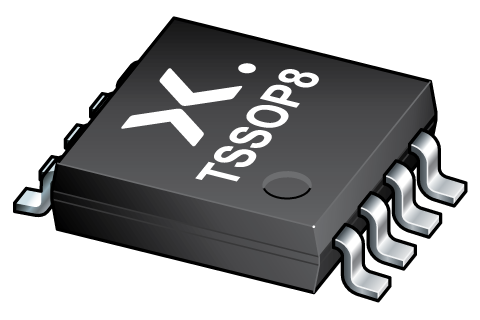 TSSOP8 (SOT505-2) | SOT505-2 | SOT505-2_125 | Active | P6 | 74HC3G16DPH ( 9353 075 77125 ) |
支持
如果您需要设计/技术支持,请告知我们并填写 应答表, 我们会尽快回复您。
订购、定价与供货
样品
安世半导体客户可通过我们的销售机构或直接通过在线样品商店订购样品: https://extranet.nexperia.com.
样品订单通常需要2-4天寄送时间。
如果您尚未取得安世半导体的直接采购帐号,我们的全球与区域经销网络可以协助您取得样品。