


74HC4017-Q100; 74HCT4017-Q100
Johnson decade counter with 10 decoded outputs
The 74HC4017-Q100; 74HCT4017-Q100 is a 5-stage Johnson decade counter with 10 decoded outputs (Q0 to Q9), an output from the most significant flip-flop (Q5-9), two clock inputs (CP0 and CP1) and an overriding asynchronous master reset input (MR). The counter is advanced by either a LOW-to-HIGH transition at CP0 while CP1 is LOW or a HIGH-to-LOW transition at CP1 while CP0 is HIGH. When cascading counters, the Q5-9 output, which is LOW while the counter is in states 5, 6, 7, 8 and 9, can be used to drive the CP0 input of the next counter. A HIGH on MR resets the counter to zero (Q0 = Q5-9 = HIGH; Q1 to Q9 = LOW) independent of the clock inputs (CP0 and CP1). Automatic code correction of the counter is provided by an internal circuit: following any illegal code the counter returns to a proper counting mode within 11 clock pulses. Inputs include clamp diodes. This enables the use of current limiting resistors to interface inputs to voltages in excess of VCC.
This product has been qualified to the Automotive Electronics Council (AEC) standard Q100 (Grade 1) and is suitable for use in automotive applications.
Features and benefits
Automotive product qualification in accordance with AEC-Q100 (Grade 1)
Specified from -40 °C to +85 °C and from -40 °C to +125 °C
Wide supply voltage range from 2.0 V to 6.0 V
CMOS low power dissipation
High noise immunity
Latch-up performance exceeds 100 mA per JESD 78 Class II Level B
Complies with JEDEC standards:
- JESD8C (2.7 V to 3.6 V)
- JESD7A (2.0 V to 6.0 V)
Input levels:
For 74HC4017-Q100: CMOS level
For 74HCT4017-Q100: TTL level
ESD protection:
HBM: ANSI/ESDA/JEDEC JS-001 class 2 exceeds 2000 V
CDM: ANSI/ESDA/JEDEC JS-002 class C3 exceeds 1000 V
Multiple package options
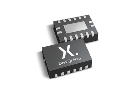
DHVQFN package with Side-Wettable Flanks enabling Automatic Optical Inspection (AOI) of solder joints
参数类型
| 型号 | VCC (V) | Output drive capability (mA) | Logic switching levels | tpd (ns) | fmax (MHz) | Power dissipation considerations | Tamb (°C) | Ψth(j-top) (K/W) | Rth(j-c) (K/W) | Package name |
|---|---|---|---|---|---|---|---|---|---|---|
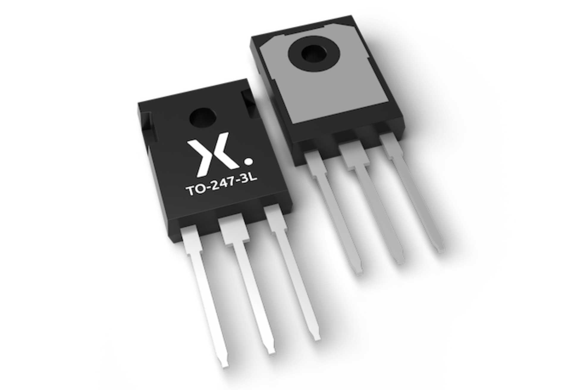
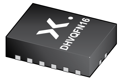
| 74HC4017BQ-Q100 | 2.0 - 6.0 | ± 5.2 | CMOS | 18 | 77 | low | -40~125 | 11.8 | 59 | DHVQFN16 |
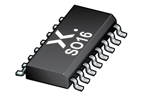
| 74HC4017D-Q100 | 2.0 - 6.0 | ± 5.2 | CMOS | 18 | 77 | low | -40~125 | 8.3 | 49 | SO16 |
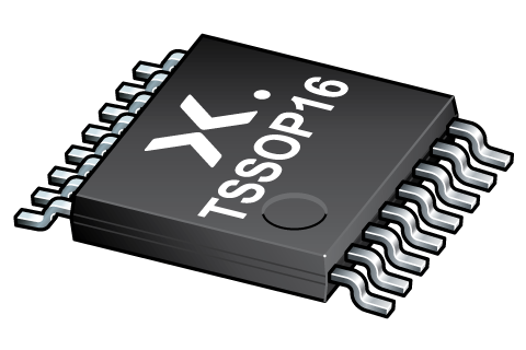
| 74HC4017PW-Q100 | 2.0 - 6.0 | ± 5.2 | CMOS | 18 | 77 | low | -40~125 | 3.9 | 51.5 | TSSOP16 |
| 74HCT4017BQ-Q100 | 4.5 - 5.5 | ± 4 | TTL | 21 | 67 | low | -40~125 | 11.8 | 59 | DHVQFN16 |
| 74HCT4017D-Q100 | 4.5 - 5.5 | ± 4 | TTL | 21 | 67 | low | -40~125 | 8.3 | 48.6 | SO16 |
封装
| 型号 | 可订购的器件编号,(订购码(12NC)) | 状态 | 标示 | 封装 | 外形图 | 回流焊/波峰焊 | 包装 |
|---|---|---|---|---|---|---|---|
| 74HC4017BQ-Q100 | 74HC4017BQ‑Q100X (935302476115) |
Active | HC4017 |
DHVQFN16 (SOT763-1) |
SOT763-1 | SOT763-1_115 | |
| 74HC4017D-Q100 | 74HC4017D‑Q100J (935302477118) |
Active | 74HC4017D |
SO16 (SOT109-1) |
SOT109-1 |
SO-SOJ-REFLOW
SO-SOJ-WAVE WAVE_BG-BD-1 |
SOT109-1_118 |
| 74HC4017PW-Q100 | 74HC4017PW‑Q100J (935302478118) |
Active | HC4017 |
TSSOP16 (SOT403-1) |
SOT403-1 |
SSOP-TSSOP-VSO-WAVE
|
SOT403-1_118 |
| 74HCT4017BQ-Q100 | 74HCT4017BQ‑Q100X (935302479115) |
Active | HT4017 |
DHVQFN16 (SOT763-1) |
SOT763-1 | SOT763-1_115 | |
| 74HCT4017D-Q100 | 74HCT4017D‑Q100J (935302481118) |
Active | 74HCT4017D |
SO16 (SOT109-1) |
SOT109-1 |
SO-SOJ-REFLOW
SO-SOJ-WAVE WAVE_BG-BD-1 |
SOT109-1_118 |
环境信息
| 型号 | 可订购的器件编号 | 化学成分 | RoHS | RHF指示符 |
|---|---|---|---|---|
| 74HC4017BQ-Q100 | 74HC4017BQ‑Q100X | 74HC4017BQ-Q100 |
|
|
| 74HC4017D-Q100 | 74HC4017D‑Q100J | 74HC4017D-Q100 |
|
|
| 74HC4017PW-Q100 | 74HC4017PW‑Q100J | 74HC4017PW-Q100 |
|
|
| 74HCT4017BQ-Q100 | 74HCT4017BQ‑Q100X | 74HCT4017BQ-Q100 |
|
|
| 74HCT4017D-Q100 | 74HCT4017D‑Q100J | 74HCT4017D-Q100 |
|
|
文档 (18)
| 文件名称 | 标题 | 类型 | 日期 |
|---|---|---|---|
| 74HC_HCT4017_Q100 | Johnson decade counter with 10 decoded outputs | Data sheet | 2024-03-27 |
| AN11044 | Pin FMEA 74HC/74HCT family | Application note | 2019-01-09 |
| AN90063 | Questions about package outline drawings | Application note | 2025-10-22 |
| SOT763-1 | 3D model for products with SOT763-1 package | Design support | 2019-10-03 |
| SOT109-1 | 3D model for products with SOT109-1 package | Design support | 2020-01-22 |
| SOT403-1 | 3D model for products with SOT403-1 package | Design support | 2020-01-22 |
| Nexperia_package_poster | Nexperia package poster | Leaflet | 2020-05-15 |
| DHVQFN16_SOT763-1_mk | plastic, dual in-line compatible thermal enhanced very thin quad flat package; 16 terminals; 0.5 mm pitch; 3.5 mm x 2.5 mm x 0.85 mm body | Marcom graphics | 2017-01-28 |
| SO16_SOT109-1_mk | plastic, small outline package; 16 leads; 1.27 mm pitch; 9.9 mm x 3.9 mm x 1.35 mm body | Marcom graphics | 2017-01-28 |
| TSSOP16_SOT403-1_mk | plastic, thin shrink small outline package; 16 leads; 0.65 mm pitch; 5 mm x 4.4 mm x 1.1 mm body | Marcom graphics | 2017-01-28 |
| SOT763-1 | plastic, leadless dual in-line compatible thermal enhanced very thin quad flat package; 16 terminals; 0.5 mm pitch; 3.5 mm x 2.5 mm x 1 mm body | Package information | 2023-05-11 |
| SOT109-1 | plastic, small outline package; 16 leads; 1.27 mm pitch; 9.9 mm x 3.9 mm x 1.75 mm body | Package information | 2023-11-07 |
| SOT403-1 | plastic, thin shrink small outline package; 16 leads; 5 mm x 4.4 mm x 1.2 mm body | Package information | 2023-11-08 |
| SO-SOJ-REFLOW | Footprint for reflow soldering | Reflow soldering | 2009-10-08 |
| HCT_USER_GUIDE | HC/T User Guide | User manual | 1997-10-31 |
| SO-SOJ-WAVE | Footprint for wave soldering | Wave soldering | 2009-10-08 |
| WAVE_BG-BD-1 | Wave soldering profile | Wave soldering | 2021-09-08 |
| SSOP-TSSOP-VSO-WAVE | Footprint for wave soldering | Wave soldering | 2009-10-08 |
支持
如果您需要设计/技术支持,请告知我们并填写 应答表 我们会尽快回复您。
Ordering, pricing & availability
样品
作为 Nexperia 的客户,您可以通过我们的销售机构订购样品。
如果您没有 Nexperia 的直接账户,我们的全球和地区分销商网络可为您提供 Nexperia 样品支持。查看官方经销商列表。