


Authors: Christian Radici, Applications Engineer, Manchester. Jae Wei, Applications Engineer, Shanghai.
This interactive application note contains embedded Cloud based simulations to augment the text.
To open the embedded simulation, simply hover over the simulation image. Left click anywhere in the graphic area once the central play button changes in colour. This opens the schematic in the Cloud environment. See the interactive application note tutorial page for more details on how to use the simulations. See accompanying application note: AN50005.
Introduction
In today's automotive and power industries, higher power requirements are leading to more designs that require lower RDSon. Sometimes this is not achievable with a single packaged MOSFET and the design will need to make use of two or more devices in parallel. Higher power applications could also require the use of high performance substrates like heavy copper PCB, IMS (Insulated Metal Substrate) or DBC (Direct Bonded Copper) and even bare dies. By paralleling, the total current and thus dissipation is shared between each device. However, this is not as simple as applying Kirchhoff's current law: MOSFETs are not identical and thus they don't share equally.
This interactive application note describes how sharing imbalances between paralleled MOSFETs form as well as guidelines and tools to take them into account. The final goal is to provide a set of best practices that can help to design circuits with standard paralleled MOSFETs.
Applications
Applications that require paralleled MOSFETs can be categorized into two main groups depending on the operation of the MOSFET: switch-mode and load switch. The switch-mode types include motor drive applications, such as belt starter generators and superchargers, braking regeneration systems and switched mode power converters, such as regulators (DC/DC) and other types of inverters (DC/AC). Here the half-bridge represents the fundamental cell block that all the major circuit topologies are based upon. The MOSFETs are generally required to switch ON and OFF at a constant rate that can vary widely depending on the application, and are driven by a rectangular pulse with varying duty cycle (PWM). This is done with the intent of modulating the output power of the system to the load.
Load switching mainly refers to applications where MOSFETs are used in series with the battery such as in activation, safety switches and e-fuses, one example being battery isolation switches. The MOSFETs are required to switch ON once and will remain fully ON until the system is switched OFF. They might be swiftly switched OFF only in case some type of failure has been detected, for example in case of short circuit. Additionally, these switches may come in a back-to-back configuration in order to offer an additional reverse polarity protection.
This interactive application note focuses on switch-mode applications and the half-bridge configuration.
Key specifications
The most important figure to monitor is the MOSFET junction temperature. This is a function of the power dissipated in each device which ideally should be uniform for all paralleled MOSFETs. Since P = V × I and the same voltage is applied across all the paralleled MOSFETs, it is clear that for ideal operation the current should be shared equally by each MOSFET and this is the simplest metric to quantify how well the MOSFETs perform. However, an equally valid approach is to consider the dissipated energy (or power), as done throughout the majority of this application note. Current sharing in paralleled MOSFETs is mainly affected by the part to part variation of three data sheet parameters: RDSon, QG(tot), and VGS(th).
Simulation 1 - Paralleled MOSFETs: ideal case
The circuit used in simulation 1 is composed of 3 MOSFETs in parallel both at the high-side and low-side driving an inductive load.
The simulation setup is as follows:
- Part name: BUK7S1R0-40H N-channel 40 V, 1.0 mΩ standard level MOSFET in LFPAK88
- VSUPPLY = 12 V
- fSW = 20 kHz
- DC = 50%
- VGS = 15 V
- ILOAD = 150 A
- LLOAD = 4 µH
Each MOSFET is conducting a current of 50 A, which is set by the constant current source of 150 A used in series with the load inductor. Parasitic inductance linked to the layout has been added to the simulation. There is no difference in terms of parasitics between the three branches (each branch corresponds to a single MOSFET and the path connecting it to the others in parallel through inlet and outlet: VSUPPLY and phase for the high-side, phase and GND for the low-side).
Simulation 1 - Paralleled MOSFETs: ideal case
MOSFET dissipation and parameters' influence on current sharing
Power dissipation in a MOSFET employed in a half-bridge is caused by two processes: conduction and switching. Fig. 1 shows the current flowing through the paralleled MOSFETs in case of ideal devices and the dissipated energy. There is no hard separation between switching and conduction losses. However, in a simulation environment, the dissipated power can help in detecting this separation.

Figure 1. MOSFETs drain current (ID) and energy dissipation (Ediss) - ideal case
Fig. 2 shows how the turn-ON phase has been found: the first point is set at around 9.9 μs where the power is 0 W, the second point is set at 10.4 μs where the dissipated power is almost constant at around 1.8 W (dissipated power during conduction - Pcond). The drain current (ID) flowing through MOSFET M1 is shown in Fig. 2, the drain-to-source voltage (VDS) across it rises before the current falls, hence the valid loss recorded here. Moreover, the increase in dissipated power starting at 10 μs and lasting around 100 ns is due to the gate charge required to turn-ON the device.

Figure 2. MOSFETs drain current (ID), energy dissipation (Ediss) and power dissipation (Pdiss) - ideal case: equal MOSFETs. The turn-ON phase is indicated
Fig. 3 shows how the turn-OFF phase has been found: the first point is set at 36.2 μs where the power is 0 W, the second point is set at around 35.2 μs where the dissipated power starts to increase from 1.8 W.

Figure 3. MOSFETs drain current (ID), energy dissipation (Ediss) and power dissipation (Pdiss) - ideal case: equal MOSFETs. The turn-OFF phase is indicated
Equation 1 expresses the power dissipation in the MOSFET, while equations 2 and 3 show the individual contributions from switching and conduction.
(Eq. 1) 
(Eq. 2) 
(Eq. 3) 
Where Esw(ON) and Esw(OFF) are the energy dissipation during turn-ON and turn-OFF, Econd is the energy dissipation during a single conduction phase and fsw the switching frequency. In this case, the total average power dissipated across each MOSFET over one cycle is around 2.1 W at 20 kHz.
Table 1 shows the energy calculated during switching (divided into ON and OFF) and conduction. The degree of sharing of each MOSFET can be defined in several ways. Here it is defined as ratio between the energy dissipated in one MOSFET and the total energy dissipated in all of the paralleled devices, by using equation 4.
(Eq. 4) 
In this case, switching (Esw(ON) + Esw(OFF)) accounts for around 55 % of the overall dissipation. However the switching:conduction dissipation ratio will depend on the switching frequency: a low frequency will lead to conduction losses dominating whereas switching losses will dominate at high frequency. Therefore, in order to simplify the evaluation, one might consider to take into account only parameters influencing the most important contribution.
With the MOSFET fully ON the only source of dissipation is given by its drain-to-source on state resistance (RDSon). On the other hand, switching depends on threshold voltage (VGS(th)) and input charge (QG(tot)).
| Device | ESW(ON) [μJ] | ESW(OFF) [μJ] | ECOND [μJ] | Total Sharing |
|---|---|---|---|---|
| M1 | 5.1 | 52.8 | 46.1 | 33% |
| M2 | 5.1 | 52.8 | 46.1 | 33% |
| M3 | 5.1 | 52.8 | 46.1 | 33% |
Influence of parameter spread on current sharing performance
As previously mentioned, manufacturing spreads in data sheet parameters have a big impact on current sharing. Spread refers to the difference between maximum and minimum of a certain parameter. These spreads are unavoidable and caused by both intra- and inter- wafer variation during the silicon die fabrication. Every MOSFET produced by any manufacturer will carry these spreads. Nexperia’s power MOSFET fabrication processes are optimised to keep spreads as tight as possible in order to achieve good performance and reliability.
Static operation (DC): drain-source on-state resistance
Fig 3. shows the BUK7S1R0 RDSon data sheet values.
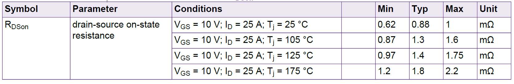
Figure 3 BUK7S1R0-40H data sheet characteristics: RDSon
The total spread, as per data sheet, is ΔRDSon = 0.38 mΩ or ΔRDSon,rel = ± 21.6 % (relative percentage with respect to the nominal value).
Simulation 2 - Paralleled MOSFETs: RDSon spread
The MOSFET having lower RDSon (M1) will need to handle more energy, vice versa for M3. Both sharing during conduction and switching are impacted. M1 is now dissipating 2.5 W, around 20% more than the ideal case (2.1 W) while M3 is dissipating 1.7 W. These results are valid only for the first cycles of operation, after which the temperature dependency of the RDSon partly balance out the sharing, more information is provided in the corresponding section on temperature dependency.
Simulation 2 - Paralleled MOSFETs: RDSon spread
| Device | RDSon [mΩ] | ESW(ON) [μJ] | ESW(OFF) [μJ] |
Energy Sharing Switching |
ECOND [μJ] | Energy Sharing Conduction |
|---|---|---|---|---|---|---|
| M1 | 0.62 | 5.0 | 65.9 | 40.7 % | 52.9 | 39.4 % |
| M2 | 0.88 | 5.1 | 48.8 | 30.9 % | 42.5 | 31.6 % |
| M3 | 1 | 5.1 | 44.3 | 28.4 % | 38.9 | 29.0 % |

Dynamic operation: total input charge – QG(tot)
Fig 3 shows the data sheet values for the typical and maximum values for gate charge parameters QG(tot), QGS and QGD; refer to Fig. 4 for definitions of these parameters.
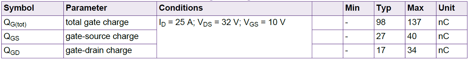
Figure 3. BUK7S1R0-40H data sheet characteristics: gate charge
The total spread, as per data sheet, is ΔQG(tot) = 39 nC or ΔQG(tot) = +40 %.
Simulation 3 - Paralleled MOSFETs: QG(tot) spread
The simulation setup and results are summarized in Table 3. At turn-ON the device with lower input capacitance (M1) will switch ON first thus handling majority of the current. On the other hand, at turn-OFF the MOSFET with higher input capacitance (M3) will switch OFF last now handling most of the current. The sharing during switching is the most impacted, while conduction has changed only marginally. M3 is now dissipating 2.8 W (0.7 W more than the ideal case) while M1 is dissipating 1.9 W.
Simulation 3 - Paralleled MOSFETs: QG(tot) spread
| Device | QG(tot) [nC] | ESW(ON) [μJ] | ESW(OFF) [μJ] |
Energy Sharing Switching |
ECOND [μJ] | Energy Sharing Conduction |
|---|---|---|---|---|---|---|
| M1 | 94.4 | 9.4 | 35.7 | 21.4 % | 49.9 | 35.8 % |
| M2 | 125.7 | 6.9 | 60.8 | 31.9 % | 46.1 | 33.2 % |
| M3 | 158 | 4.7 | 94.4 | 46.7 % | 43.2 | 31.0 % |
Dynamic operation: gate-source threshold voltage – VGS(th)
Fig 4 shows the data sheet values for gate-source threshold voltage.
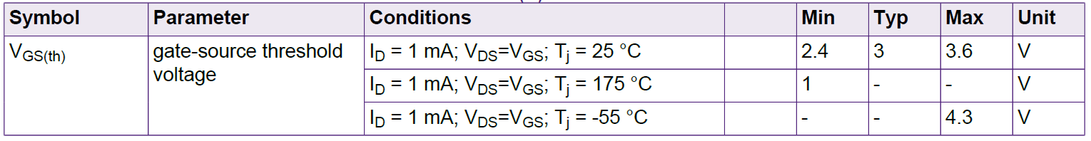
Figure 4. BUK7S1R0-40H data sheet characteristics: gate-source threshold voltage
The total spread, as per data sheet, is ΔVGS(th) = 1.2 V or ΔVGS(th)rel = ±20 %.
Simulation 4 - Paralleled MOSFETs: VGS(th)data sheet spread
The simulation setup and results are summarized in Table 3. The MOSFET having lower VGS(th) will need to handle more energy overall. At turn-ON M1 will switch ON first thus handling majority of the current. Moreover, at turn-OFF the same MOSFET will switch OFF last, again, handling most of the current. The sharing during switching is the most impacted, with one MOSFET (M3) participating only minimally in the process, while conduction has changed only marginally. M1 is now dissipating 4.7 W (2.6 W more than the ideal case) while M3 only 1 W.
Simulation 4 - Paralleled MOSFETs: VGS(th) spread
| Device | VGS(th) [V] | ESW(ON) [μJ] | ESW(OFF) [μJ] |
Energy Sharing Switching |
ECOND [μJ] | Energy Sharing Conduction |
|---|---|---|---|---|---|---|
| M1 | 2.4 | 9.3 | 172.2 | 74.4 % | 52.7 | 37.8 % |
| M2 | 3 | 5.1 | 48.7 | 22.1 % | 45.7 | 33.8 % |
| M3 | 3.6 | 2.2 | 6.4 | 3.5 % | 40.8 | 29.4 % |
In conclusion, the MOSFET having lower VGS(th) will need to handle more energy both during turn-ON and turn-OFF, while with the capacitance spread the switching energy will be balanced between at least two devices. These results are valid only for the first cycles of operation, due to the temperature dependency of the VGS(th). More information is provided in the corresponding section on temperature dependency.

Paralleled MOSFETs and temperature dependency
Each MOSFET can be thought as a system composed of an electrical subsystem in a feedback loop with a thermal subsystem, as shown in Fig. 5. Power MOSFETs are often considered to be immune to thermal runaway due to the RDSon temperature coefficient. However, this is only true for MOSFETs that are fully ON. When a MOSFET is in the on-state, there are two competing effects that determine how its current behaves with increasing temperature.

As the temperature rises, VGS(th) falls, thereby increasing the current. On the other hand, RDSon increases with increasing temperature, thereby reducing the current. The resistance increase dominates at higher gate-source voltages (VGS),while the threshold-voltage drop dominates at low VGS. Consequently, for a given VDS, there is a critical VGS below which there is a positive feedback regime and above which there is a negative feedback and thermal stability. This critical point is known as the Zero Temperature Coefficient (ZTC) point, Fig. 6..

Temperature dependency during static operation (DC)
In a parallel configuration, RDSon has the advantage of improving the sharing due to its positive temperature coefficient (PTC), Fig. 7.
As one MOSFET conducts more current and dissipates more power, RDSon increases and the conduction losses change improving the sharing.
Ideally this phenomenon is maximized when the thermal coupling between paralleled MOSFETs is less effective, as each MOSFET is less influenced by the others around it. However, this leads to higher junction temperatures.

Temperature dependency during dynamic operation
Threshold voltage is characterized by a negative temperature coefficient (NTC): it decreases as the junction temperature increases. This behaviour is more detrimental in case of paralleled MOSFETs. For instance, a device with an initial higher junction temperature will exhibit an even lower VGS(th) which increases the current flowing through the MOSFET and thus the power that it dissipates. As in the static case, good thermal coupling helps to keep the MOSFETs at similar temperatures. Other guidelines could be adopted to mitigate temperature gradient across paralleled MOSFETs.
Fig. 8 shows how the VGS(th) spread is almost constant with respect to the junction temperature, however this behaviour is guaranteed only at a drain current of 1 mA. For a temperature difference of 20 °C (from 25 to 45 °C) VGS(th) reduces by about 0.2 V.
Finally, unlike RDSon and VGS(th), input charge is shown to only slightly vary with temperature.
Data sheet and batch spreads
If considering multiple MOSFETs in parallel, data sheet spreads may be too conservative. The design would certainly be reliable but the improved robustness to a wider worst case scenario could end up being more expensive. In this case then, the designer would prefer to evaluate a less stringent worst case scenario that, even if not guaranteed like the data sheet, can still be considered realistic. This is done by looking at batch spreads.
A batch refers to a group of devices that go through the whole manufacturing process at the same time. The number of dies in a batch can vary from a few thousands to over a few millions, depending on the size of the dies themselves. Within a set of paralleled MOSFETs, it is preferable to choose parts coming from the same reel in order to increase the possibility of using devices from the same batch. Furthermore, using MOSFETs with identical batch codes, which can be found on the package under the marking code, could be used to further narrow down the selection during PCB assembly.
Spreads within a batch are observed to be much lower than the corresponding data sheet ones.The same can be said even with those among different batches. Fig. 9 shows the spread of VGS(th) for the BUK7S1R5-40H for 10 different batches. In this case the 6-sigma spread is observed to be 0.42 V, from 2.86 V to 3.28 V. This value is calculated taking into account a small quantity of outliers (not shown in the plot of Fig. 9). Therefore, the observed worst case is given by a ΔVGS(th) = 0.42 V or ΔVGS(th),rel = ± 7 %, less than half of the guaranteed (data sheet) one.

Figure 9. VGS(th) batches spread for BUK7S1R5-40H

Fig. 10 shows the absolute value of the difference in VGS(th) (|ΔVGS(th)|) between two consecutive devices, within two different batches. In this case the 6-sigma spread is observed to be 0.25 V, or ΔVGS(th) = ±4 %. Therefore, in case two consecutive MOSFETs coming from the same reel are used in parallel, the difference between their VGS((th),rel is observed to be even smaller than that between multiple batches.
Simulation 5 compares the MOSFETs drain current in case of data sheet and batch spread, Table 4 quotes the energy shared by each MOSFET. M1 is now dissipating a total of 2.8 W and M3 1.5 W. Therefore, a difference of ±7 % in VGS(th) leads to a reduction of 1.9 W over a cycle of M1, reducing the ratio between these two MOSFETs dissipation from almost 5:1 down to 2.5:1.
Simulation 5 - Paralleled MOSFETs: VGS(th) (data sheet vs. batch) spread
Simulation 5. Paralleled MOSFETs: VGS(th) (data sheet vs batch) Spread.
| Device | VGS(th) [V] | ESW [μJ] | Energy Sharing Switching |
ECOND [μJ] | Energy Sharing Conduction |
|---|---|---|---|---|---|
| M1 | 2.79 | 97 | 51.3 % | 48.7 | 35.6 % |
| M2 | 3 | 59.4 | 31.4 % | 45.4 | 33.2 % |
| M3 | 3.21 | 32.6 | 17.2 % | 42.7 | 31.2 % |
Circuit optimisation
There are different types of circuit modifications, each has a different impact on the current sharing. In the following section only one will be discussed, due to its most advantageous aspects.
Localized gate resistor
This type of circuit modification is the most advantageous, it has no major drawbacks and it is the simplest to implement. The modification involves splitting the gate resistor between a localized one close to the gate of each MOSFET and a common resistor at the driver side, as shown in Fig. 11 b. Doing so will counteract the spreads and improve the sharing, mainly during switching with little impact during conduction. It is important to keep the localized resistance as low as possible to give maximum coupling between the MOSFET gates, effectively allowing the input capacitances to be considered in parallel. A simple simulation can display this effect: two circuits modelling the driver and input impedance of each MOSFET are used as comparison. Fig. 11 a. shows the control voltage at each MOSFET gate, the voltage is slowed down in case of the MOSFET with higher Ciss, vice versa it is less filtered in case of lower capacitance. By splitting the gate resistor the difference between the control voltages at each gate becomes negligible (Fig. 11 b).

Figure 11. SPICE simulation circuit: gate resistor split comparison
With reference to the naming adopted in the SPICE circuits of Fig. 11, the gate resistor at the driver can be calculated as:
(Eq. 5) 
The value of RG,drv has been rounded to 12 Ω. A smaller RG,drv can be beneficial by reducing the switching time where the unequal sharing occurs. In a similar manner, the smaller RG,split the better coupled the MOSFETs gate, but it is recommended not to go below 2-3 Ω. In general, a gate resistor helps in dampening any oscillation in the gate-source loop that might compromise the EMC performance of the system. Therefore, given a lower resistance of the gate resistor, it is important to reduce as much as possible the loop inductance of the driver loop.
The great improvement of the resistor split can be easily appreciated by simulating the same half-bridge circuit using two different gate resistors setups and introducing some spread. This time an arbitrary combination of all the spreads has been used.

Figure 12. Gate-source voltage without and with gate resistor split
Simulation 6 - Paralleled MOSFETs: gate resistor split
Simulation 6. Paralleled MOSFETs: Gate Resistor Split
The simulations setup and results are summarized in Table 5 and Table 6, while a final comparison is given in Table 7. M3 is dissipating 8.2 W, M2 1.3 W and M1 2.0 W. At turn-ON M1 is switching first, due to having both lower QG(tot) and VGS(th), thus handling the majority of the current. On the other hand, at turn-OFF the MOSFET with higher input charge (M3) will switch last and carry most of the current.
| Device | RDSon [mΩ] | VGS(th) [V] | QGS(tot) [nC] | ESW [μJ] | Energy Sharing Switching |
ECOND [μJ] | Energy Sharing Conduction |
|---|---|---|---|---|---|---|---|
| M1 | 0.62 | 3.21 | 94.4 | 42.7 | 9.6 % | 62.2 | 47.0 % |
| M2 | 1 | 3 | 125.7 | 29 | 6.5 % | 35.2 | 26.6 % |
| M3 | 0.88 | 2.79 | 158 | 373 | 83.9 % | 34.9 | 25.4 % |
With the gate resistor split M3 is now dissipating 3.8 W, M2 2.0 W and M1 1.6 W. The improvements are noticeable both at turn-ON, where the peaks are now almost identical, and turn-OFF. Sharing during conduction has improved as well, this is due to time it takes for the current to reach its conduction value following the turn-ON event. Overall, M3 is now dissipating 50 % less power.
| Device | RDSon [mΩ] | VGS(th) [V] | QGS(tot) [nC] | ESW [μJ] | Energy Sharing Switching |
ECOND [μJ] | Energy Sharing Conduction |
|---|---|---|---|---|---|---|---|
| M1 | 0.62 | 3.21 | 94.4 | 30 | 12.4 % | 52.3 | 39.6 % |
| M2 | 1 | 3 | 125.7 | 60.6 | 25.1 % | 38.2 | 28.9 % |
| M3 | 0.88 | 2.79 | 158 | 150.5 | 62.4 % | 41.4 | 31.5 % |
| Device | Total Energy Sharing without gate resistor split |
Total Energy Sharing with gate resistor split |
|---|---|---|
| M1 | 18.1 % | 22.1 % |
| M2 | 11.12 % | 26.5 % |
| M3 | 70.7 % | 51.4 % |
PCB layout influence
Tight spreads and a good layout are two important factors when designing an application with paralleled MOSFETs. This section describes guidelines to achieve a good layout and how parasitics influence the current sharing.
In a paralleled set of MOSFETs it is impossible to say beforehand where the device with lowest or highest spreads will be placed. Therefore, it is important to lay out each branch in the same way, failing to do so will result in the worsening of the worst case scenario.
Layout-dependent parasitics
In case of paralleled devices loop inductance and resistance in the path should be not only minimised but also equalised for each branch.
Higher inductance slows down the current reaching its steady state value due to the higher time constant of the circuit (τ = L/R), as shown in Fig. 13. The inductance decreases the peak current slightly but increases the overall sharing unbalance.

Figure 13. MOSFETs drain current (ID) - effects of parasitic inductance

Moreover, both high and low sides will experience larger voltage overshoots and oscillations in VDS (and VGS) due to resonance with the capacitances in the circuit (Fig. 14), often exceeding the supply voltage. This also leads to higher interference with nearby circuits and wiring.
In general, any rule that would be recommended for a single MOSFET can be applied here. For a more in depth explanation of the switching behaviour of a half-bridge and EMC consideration refer to: AN90011: Half-bridge MOSFET switching and its impact on EMC.
Differences between loop inductances lead to worse current sharing, as shown in Fig. 15.

Figure 15. MOSFETs drain current (ID) - effects of parasitic inductance imbalance
Circuit PCB layout
Electronic system, almost as much as the quality of the parts. In case of paralleled MOSFETs the layout should be designed to provide: good thermal link between the devices, low and equal loop inductance in the gate-source and source-drain loops and low and equal resistance between the branches.
Good thermal coupling allows the devices to operate at similar lower temperatures. Furthermore, the designer should aim at obtaining similar Rth(mb-amb)for each MOSFET. Multiple planes and thermal vias help in improving the heat exchange between devices and environment. Care should be taken in the placement of the MOSFETs: for instance by avoiding placing a subset of the MOSFETs near heat sinks, connectors or other components that may be keep them cooler than the other paralleled MOSFETs. For more information about this topic refer to AN90003: LFPAK MOSFET thermal design guide.

Low inductance in a loop can be achieved by reducing the area of the loop (thereby reducing the self-inductance) or by keeping the trace and its return path as close as possible to each other (thereby increasing the mutual inductance). Loop inductance in the gate-source loop can be reduced by keeping the driver as close as possible to the MOSFETs and by running gate and source traces parallel to each other, as shown in Fig. 16.
Inductance in the loop carrying the load current could be minimised, for instance, by employing the design in Fig. 17.
For further details refer to: AN90011: Half-bridge MOSFET switching and its impact on EMC.

The placement of inlets and outlets plays another important role because it determines each branch parasitics. When using multiple devices in parallel, it could be helpful to use more than one inlet and outlet. Using multiple smaller cables can be actually beneficial for other reasons too. The positioning of these insertion points needs to be carefully planned.
One possible way to facilitate this decision might be to use a CFD software and run a current density simulation. This type of simulation highlights the preferred path the current takes in a steady state condition (DC).
Fig. 18 shows the setup used for the simulations: 3 MOSFETs are placed in parallel both at high and low side. Each low side MOSFET is connected between phase (inlet), on the top layer, and ground (outlet) on the bottom one (not shown in the picture), through a number of filled vias. Each high side is instead connected between phase (outlet) and the positive supply (inlet) on the top layer. A total current of 150 A is set to flow through the paralleled devices.
Two simulations are required, each with a single side active at a time.

Figure 18. CFD simulation setup
The results of the current density simulation for the low side and high side are shown in Fig. 19. Higher current density is shown in red, while low or null in blue. For instancethe high side simulation highlights a spot around M4 and inlet VBUS1 where current density is higher, due to the position of the latter. By integrating the current density over the entire surface of the die it is possible to calculate the sharing in steady state of the layout (between 30-40% in this particular case). These simulations have been obtained using scSTREAM.


Figure 19. CFD current density simulation: Low side MOSFETs ON – Top side, Low side MOSFETs ON – Bottom side, High side MOSFETs ON – Top side
Driving paralleled MOSFETs
When driving paralleled MOSFETs it is recommended to use one single gate driver. This is mainly done to synchronize the devices operation as much as possible.
The gate driver should have enough peak current capability to fully charge and discharge the total input capacitance of the paralleled MOSFETs. This requirement becomes more and more stringent as the number of MOSFETs increases, especially if the switching time is required to be low, as the total input capacitance is now Ciss,= n.FETs × Ciss,max. Failing to do so means that the switching tot speed will be set by the gate driver itself and not by the gate resistor.

As shown by the previous simulations turn-OFF dissipates more energy than turn-ON. One simple way to reduce the switching losses is by decreasing the resistance of RG,drv only during the turn-OFF.
This can be done by using a combination of a smaller resistor in series with a diode, placedin parallel with RG,drv, as shown in Fig. 20. However, before choosing the right value of RG,OFF it is recommended to take into account any parasitic inductance that may be present in the circuit: a combination of fast turn-OFF and high inductance could potentially induce avalanche, which, in a parallel configuration, could greatly stress the device with lower breakdown voltage.
Summary
This interactive application note aims to give the reader a description of how the sharing among paralleled MOSFETs is influenced by parameters spreads (e.g. RDSon, VGS(th) and QG(tot)) and PCB layout. The analysis is conducted considering switch-mode (PWM) applications and thus the half-bridge topology.
During switching, VGS(th) spread contributes the most to current unbalances, affecting turn-ON and turn-OFF in the same way: the device with lower VGS(th) will turn-ON first and turn-OFF last, dissipating more power during both events. Additionally, the NTC of VGS(th) leads to increased dissipation as it further lowers the VGS(th) of the MOSFET that handles more power. The spread in QG(tot) can be effectively counteracted by splitting the gate resistor between one close to the MOSFETs gate and a common one at the driver side. This modification will improve the sharing with huge benefits during switching.
The RDSon is not as significant as VGS(th) when considering MOSFETs in parallel since its PTC improves the sharing during conduction and counteracts the imbalances caused by RDSon spread. Additionally the losses during conduction (I2 × R) are generally lower than the switching losses therefore the imbalance will weigh less on the overall power sharing.
A worst case scenario simulation can be used to quantify and evaluate the performance of paralleled devices. It can be useful to understand which and how many devices to use in parallel. The worst case depends mainly on the spread of certain parameters. The VGS(th) batch variability is shown to be around half that indicated on the respective data sheet. Albeit not guaranteed, spread between batches is more realistic and leads to a design with improved performance.
How to parallel power MOSFETs – Quick Learning
How to parallel power MOSFETs – Quick Learning
| Page last updated 16 November 2021. |