


NPS1001
0.5 V to 1.8 V, 1.5 A peak, 12 mΩ, load switch
NPS1001 is a low voltage, single-channel load switch with a low RDS,ON (12 mΩ) to minimize IR drop and power loss. It supports up to 0.6 A RMS current and a peak current of 1.5 A.
The switch is controlled by an enable input (EN) which is compatible with 1.2 V logic levels. When the load switch is enabled, the internal switch charges the output capacitor with a controlled inrush current. When the switch is disabled, an 8 Ω on-chip resistor discharges the output to ground and keeps it from floating.
The IC is powered from a separate BIAS pin which is rated for 3 V to 5 V operation.
NPS1001 has an over-temperature protection that latches the device OFF when the internal junction temperature is above the set point (Tth(OTLO)). At this time, the internal switch is turned off and the output discharge element turns on to discharge the output capacitor. The load switch can be enabled again by toggling the enable (EN) pin.
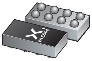
NPS1001 is available in an ultra-small, space saving, wafer level chip-scale package; 8 bumps; 1.42 mm × 0.72 mm × 0.465 mm body and is characterized for operation over ambient temperature range of –40 °C to 105 °C.

Features and benefits
- 0.5 V to 1.8 V operation voltage
- 3 V to 5 V bias voltage
- Low RDS,ON: 12 mΩ (typical) at 25 °C, 16 mΩ (maximum) at 85 °C
- Enable logic supports 1.2 V logic levels
- 0.6 A RMS and 1.5 A peak current capability
- Controlled start-up
- <200 µs from enable to full enhancement of power FET
- Output short tolerant
- When supplied by a 4.5 A current limited power supply
- Over-temperature shutdown and input UVLO protection
- 8 Ω discharge while disabled
- Small package footprint
ESD protection:
HBM: ANSI/ESDA/JEDEC JS-001 class 2 exceeds 2000 V
CDM: ANSI/ESDA/JEDEC JS-002 class C2a exceeds 500 V
Specified from Tj = -40 °C to +105 °C
Applications
Mobile phones
Wearables
封装
| 型号 | 可订购的器件编号,(订购码(12NC)) | 状态 | 标示 | 封装 | 外形图 | 回流焊/波峰焊 | 包装 |
|---|---|---|---|---|---|---|---|
| NPS1001UP | NPS1001UPZ (935692138336) |
Active | sD |
(WLCSP8_SOT8068) |
WLCSP8_SOT8068 | 暂无信息 |
文档 (3)
| 文件名称 | 标题 | 类型 | 日期 |
|---|---|---|---|
| NPS1001 | 0.5 V to 1.8 V, 1.5 A peak, 12 mΩ, load switch | Data sheet | 2024-12-09 |
| AN90063 | Questions about package outline drawings | Application note | 2025-10-22 |
| WLCSP8_SOT8068 | wafer level chip-scale package; 8 bumps; 1.42 × 0.72 × 0.465 mm body | Package information | 2024-01-25 |
支持
如果您需要设计/技术支持,请告知我们并填写 应答表 我们会尽快回复您。
模型
No documents available