
特性
-
Automotive product qualification in accordance with AEC-Q100 (Grade 1)
-
Specified from -40 °C to +85 °C and from -40 °C to +125 °C
-
-
Wide supply voltage range from 0.8 V to 3.6 V
-
High noise immunity
-
Low static power consumption; ICC = 0.9 μA (maximum)
-
Latch-up performance exceeds 100 mA per JESD78 Class II
-
Inputs accept voltages up to 3.6 V
-
Low noise overshoot and undershoot < 10 % of VCC
-
IOFF circuitry provides partial Power-down mode operation
-
Complies with JEDEC standards:
-
JESD8-12 (0.8 V to 1.3 V)
-
JESD8-11 (0.9 V to 1.65 V)
-
JESD8-7 (1.2 V to 1.95 V)
-
JESD8-5 (1.8 V to 2.7 V)
-
JESD8-B (2.7 V to 3.6 V)
-
-
ESD protection:
-
HBM: ANSI/ESDA/JEDEC JS-001 class 3A exceeds 5000 V
-
CDM: ANSI/ESDA/JEDEC JS-002 class C3 exceeds 1000 V
-
参数类型
| Type number | Product status | VCC (V) | Logic switching levels | Output drive capability (mA) | tpd (ns) | fmax (MHz) | Power dissipation considerations | Tamb (°C) | Rth(j-a) (K/W) | Ψth(j-top) (K/W) | Rth(j-c) (K/W) | Package name |
|---|---|---|---|---|---|---|---|---|---|---|---|---|
| 74AUP2G80DC-Q100 | Production | 0.8 - 3.6 | CMOS | ± 1.9 | 9.1 | 400 | ultra low | -40~125 | 203 | 34.1 | 113 | VSSOP8 |
封装
| 型号 | 封装 | 尺寸版本 | 回流焊/波峰焊 | 包装 | 状态 | 标示 | 可订购的器件编号,(订购码(12NC)) |
|---|---|---|---|---|---|---|---|
| 74AUP2G80DC-Q100 | 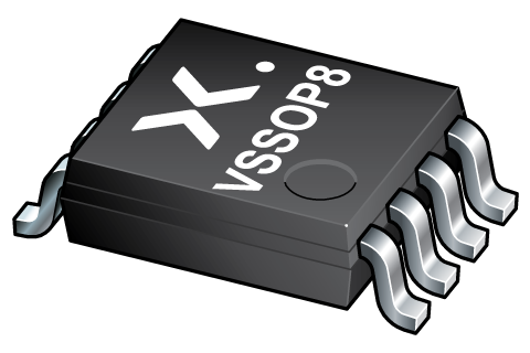 VSSOP8 (SOT765-1) | SOT765-1 | SOT765-1_125 | Active | p80 | 74AUP2G80DC-Q100H ( 9356 915 78125 ) |
文档 (2)
| 文件名称 | 标题 | 类型 | 日期 |
|---|---|---|---|
| 74AUP2G80_Q100 | Low-power dual D-type flip-flop; positive-edge trigger | Data sheet | 2023-10-16 |
| SOT765-1 | plastic, very thin shrink small outline package; 8 leads; 0.5 mm pitch; 2 mm x 2.3 mm x 1 mm body | Package information | 2022-06-03 |
支持
如果您需要设计/技术支持,请告知我们并填写 应答表, 我们会尽快回复您。
订购、定价与供货
样品
安世半导体客户可通过我们的销售机构或直接通过在线样品商店订购样品: https://extranet.nexperia.com.
样品订单通常需要2-4天寄送时间。
如果您尚未取得安世半导体的直接采购帐号,我们的全球与区域经销网络可以协助您取得样品。