
参数类型
| 型号 | VCC (V) | Logic switching levels | Output drive capability (mA) | tpd (ns) | fmax (MHz) | Power dissipation considerations | Tamb (°C) | Rth(j-a) (K/W) | Ψth(j-top) (K/W) | Rth(j-c) (K/W) | Package name |
|---|---|---|---|---|---|---|---|---|---|---|---|
| 74LVC74ABQ-Q100 | 1.2 - 3.6 | CMOS/LVTTL | ± 24 | 2.5 | 250 | low | -40~125 | 107 | 21.7 | 75 | DHVQFN14 |
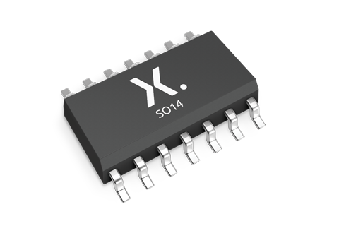
| 74LVC74AD-Q100 | 1.2 - 3.6 | CMOS/LVTTL | ± 24 | 2.5 | 250 | low | -40~125 | 109 | 21 | 68 | SO14 |
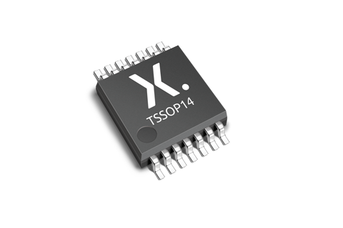
| 74LVC74APW-Q100 | 1.2 - 3.6 | CMOS/LVTTL | ± 24 | 2.5 | 250 | low | -40~125 | 142 | 8.1 | 68 | TSSOP14 |
封装
| 型号 | 可订购的器件编号,(订购码(12NC)) | 状态 | 标示 | 封装 | 外形图 | 回流焊/波峰焊 | 包装 |
|---|---|---|---|---|---|---|---|
| 74LVC74ABQ-Q100 | 74LVC74ABQ-Q100X (935301368115) |
Active | VC74A |
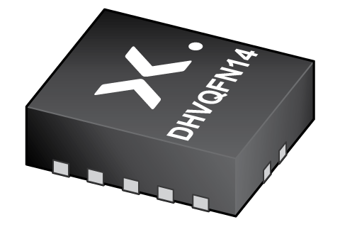
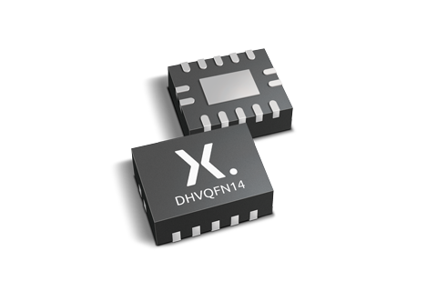
DHVQFN14 (SOT762-1) |
SOT762-1 | SOT762-1_115 | |
| 74LVC74AD-Q100 | 74LVC74AD-Q100J (935300463118) |
Active | 74LVC74AD |
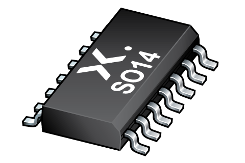
SO14 (SOT108-1) |
SOT108-1 |
SO-SOJ-REFLOW
SO-SOJ-WAVE WAVE_BG-BD-1 |
SOT108-1_118 |
| 74LVC74APW-Q100 | 74LVC74APW-Q100J (935300464118) |
Active | LVC74A |
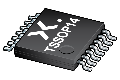
TSSOP14 (SOT402-1) |
SOT402-1 |
SSOP-TSSOP-VSO-WAVE
|
SOT402-1_118 |
环境信息
| 型号 | 可订购的器件编号 | 化学成分 | RoHS | RHF指示符 |
|---|---|---|---|---|
| 74LVC74ABQ-Q100 | 74LVC74ABQ-Q100X | 74LVC74ABQ-Q100 |
|
|
| 74LVC74AD-Q100 | 74LVC74AD-Q100J | 74LVC74AD-Q100 |
|
|
| 74LVC74APW-Q100 | 74LVC74APW-Q100J | 74LVC74APW-Q100 |
|
|
文档 (20)
| 文件名称 | 标题 | 类型 | 日期 |
|---|---|---|---|
| 74LVC74A_Q100 | Dual D-type flip-flop with set and reset; positive-edge trigger | Data sheet | 2024-02-22 |
| AN11009 | Pin FMEA for LVC family | Application note | 2019-01-09 |
| AN263 | Power considerations when using CMOS and BiCMOS logic devices | Application note | 2023-02-07 |
| AN90063 | Questions about package outline drawings | Application note | 2025-03-12 |
| SOT762-1 | 3D model for products with SOT762-1 package | Design support | 2019-10-03 |
| SOT108-1 | 3D model for products with SOT108-1 package | Design support | 2020-01-22 |
| SOT402-1 | 3D model for products with SOT402-1 package | Design support | 2023-02-02 |
| lvc74a | lvc74a IBIS model | IBIS model | 2013-04-09 |
| Nexperia_package_poster | Nexperia package poster | Leaflet | 2020-05-15 |
| DHVQFN14_SOT762-1_mk | plastic, dual in-line compatible thermal enhanced very thin quad flat package; no leads; 14 terminals; 0.5 mm pitch; 2.5 mm x 3 mm x 0.85 mm body | Marcom graphics | 2017-01-28 |
| SO14_SOT108-1_mk | plastic, small outline package; 14 leads; 1.27 mm pitch; 8.65 mm x 3.9 mm x 1.75 mm body | Marcom graphics | 2017-01-28 |
| TSSOP14_SOT402-1_mk | plastic, thin shrink small outline package; 14 leads; 0.65 mm pitch; 5 mm x 4.4 mm x 1.1 mm body | Marcom graphics | 2017-01-28 |
| SOT762-1 | plastic, leadless dual in-line compatible thermal enhanced very thin quad flat package; 14 terminals; 0.5 mm pitch; 2.5 x 3 x 1 mm body | Package information | 2023-04-05 |
| SOT108-1 | plastic, small outline package; 14 leads; 1.27 mm pitch; 8.65 mm x 3.9 mm x 1.75 mm body | Package information | 2023-11-07 |
| SOT402-1 | plastic, thin shrink small outline package; 14 leads; 0.65 mm pitch; 5 mm x 4.4 mm x 1.2 mm body | Package information | 2023-11-07 |
| SO-SOJ-REFLOW | Footprint for reflow soldering | Reflow soldering | 2009-10-08 |
| lvc | lvc Spice model | SPICE model | 2013-05-07 |
| SO-SOJ-WAVE | Footprint for wave soldering | Wave soldering | 2009-10-08 |
| WAVE_BG-BD-1 | Wave soldering profile | Wave soldering | 2021-09-08 |
| SSOP-TSSOP-VSO-WAVE | Footprint for wave soldering | Wave soldering | 2009-10-08 |
支持
如果您需要设计/技术支持,请告知我们并填写 应答表 我们会尽快回复您。
模型
| 文件名称 | 标题 | 类型 | 日期 |
|---|---|---|---|
| SOT762-1 | 3D model for products with SOT762-1 package | Design support | 2019-10-03 |
| SOT108-1 | 3D model for products with SOT108-1 package | Design support | 2020-01-22 |
| SOT402-1 | 3D model for products with SOT402-1 package | Design support | 2023-02-02 |
| lvc74a | lvc74a IBIS model | IBIS model | 2013-04-09 |
| lvc | lvc Spice model | SPICE model | 2013-05-07 |
Ordering, pricing & availability
样品
作为 Nexperia 的客户,您可以通过我们的销售机构订购样品。
如果您没有 Nexperia 的直接账户,我们的全球和地区分销商网络可为您提供 Nexperia 样品支持。查看官方经销商列表。