

NXS0102
Dual supply translating transceiver; open drain; auto direction sensing
The NXS0102 is a 2-bit, dual supply translating transceiver with auto direction sensing, that enables bidirectional voltage level translation. It features two 2-bit input-output ports (An and Bn), one output enable input (OE) and two supply pins (VCC(A) and VCC(B)). VCC(A) can be supplied at any voltage between 1.65 V and 3.6 V and VCC(B) can be supplied at any voltage between 2.3 V and 5.5 V, making the device suitable for translating between any of the voltage nodes (1.8 V, 2.5 V, 3.3 V and 5.0 V). Pins An and OE are referenced to VCC(A) and pins Bn are referenced to VCC(B). A LOW level at pin OE causes the outputs to assume a high-impedance OFF-state. This device is fully specified for partial power-down applications using IOFF. The IOFF circuitry disables the output, preventing the damaging backflow current through the device when it is powered down.
Features and benefits
Wide supply voltage range:
VCC(A): 1.65 V to 3.6 V and VCC(B): 2.3 V to 5.5 V
Maximum data rates:
Push-pull: 24 Mbps
IOFF circuitry provides partial Power-down mode operation
Inputs accept voltages up to 5.5 V
Latch-up performance exceeds 100 mA per JESD 78B Class II
ESD protection:
HBM: ANSI/ESDA/JEDEC JS-001 class 2 exceeds 2500 V for A port
HBM: ANSI/ESDA/JEDEC JS-001 class 3B exceeds 8000 V for B port
CDM: ANSI/ESDA/JEDEC JS-002 class C3 exceeds 1500 V
Multiple package options
Specified from -40 °C to +85 °C and -40 °C to +125 °C
Applications
Desktop PC
Handset
Smartphone
Tablet
参数类型
| 型号 | VCC(A) (V) | VCC(B) (V) | Logic switching levels | Output drive capability (mA) | tpd (ns) | Nr of bits | Power dissipation considerations | Tamb (°C) | Rth(j-a) (K/W) | Ψth(j-top) (K/W) | Rth(j-c) (K/W) | Package name | Category |
|---|---|---|---|---|---|---|---|---|---|---|---|---|---|
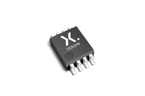
| NXS0102DC | 1.65 - 3.6 | 2.3 - 5.5 | CMOS | - 0.02 / 1.0 | 5.2 | 2 | low | -40~125 | 169 | 10.6 | 76 | VSSOP8 | Bidirectional | AutoSense |
| NXS0102GT | 1.65 - 3.6 | 2.3 - 5.5 | CMOS | - 0.02 / 1.0 | 5.2 | 2 | low | -40~125 | 169 | 10.6 | 76 | XSON8 | Bidirectional | AutoSense |
| NXS0102UN | 1.65 - 3.6 | 2.3 - 5.5 | CMOS | - 0.02 / 1.0 | 5.2 | 2 | low | -40~125 | 139 | 12 | WLCSP8 | Bidirectional | AutoSense |
封装
| 型号 | 可订购的器件编号,(订购码(12NC)) | 状态 | 标示 | 封装 | 外形图 | 回流焊/波峰焊 | 包装 |
|---|---|---|---|---|---|---|---|
| NXS0102DC | NXS0102DC/GH (935693439125) |
Development | m2 |

VSSOP8 (SOT765-1) |
SOT765-1 | SOT765-1_125 | |
| NXS0102DCH (935690905125) |
Active | m2 | SOT765-1_125 | ||||
| NXS0102GT | NXS0102GTX (935690913115) |
Active | m2 |

XSON8 (SOT833-1) |
SOT833-1 | SOT833-1_115 | |
| NXS0102UN | NXS0102UNAZ (935691106336) |
Active | m2 |

WLCSP8 (SOT8023-1) |
SOT8023-1 | SOT8023-1_336 |



文档 (15)
| 文件名称 | 标题 | 类型 | 日期 |
|---|---|---|---|
| NXS0102 | Dual supply translating transceiver; open drain; auto direction sensing | Data sheet | 2023-11-16 |
| AN90014 | Pin FMEA for NXS family | Application note | 2020-03-25 |
| AN90063 | Questions about package outline drawings | Application note | 2026-06-17 |
| Nexperia_document_guide_MiniLogic_PicoGate_201901 | PicoGate leaded logic portfolio guide | Brochure | 2019-01-07 |
| Nexperia_document_guide_MiniLogic_MicroPak_201808 | MicroPak leadless logic portfolio guide | Brochure | 2018-09-03 |
| SOT765-1 | 3D model for products with SOT765-1 package | Design support | 2020-01-22 |
| SOT833-1 | 3D model for products with SOT833-1 package | Design support | 2021-01-28 |
| SOT8023-1 | 3D model for products with SOT8023-1 package | Design support | 2023-02-07 |
| nxs0102 | NXS0102 IBIS model | IBIS model | 2020-11-05 |
| Nexperia_package_poster | Nexperia package poster | Leaflet | 2020-05-15 |
| VSSOP8_SOT765-1_mk | plastic, very thin shrink small outline package; 8 leads; 0.5 mm pitch; 2 mm x 2.3 mm x 1 mm body | Marcom graphics | 2017-01-28 |
| SOT765-1 | plastic, very thin shrink small outline package; 8 leads; 0.5 mm pitch; 2 mm x 2.3 mm x 1 mm body | Package information | 2022-06-03 |
| SOT833-1 | plastic, leadless extremely thin small outline package; 8 terminals; 0.5 mm pitch; 1 mm x 1.95 mm x 0.5 mm body | Package information | 2022-06-03 |
| SOT8023-1 | wafer level chip-scale package, 8 bumps; 0.75 x 1.55 x 0.60 mm | Package information | 2022-04-20 |
| MAR_SOT833 | MAR_SOT833 Topmark | Top marking | 2013-06-03 |
支持
如果您需要设计/技术支持,请告知我们并填写 应答表 我们会尽快回复您。
模型
| 文件名称 | 标题 | 类型 | 日期 |
|---|---|---|---|
| SOT765-1 | 3D model for products with SOT765-1 package | Design support | 2020-01-22 |
| SOT833-1 | 3D model for products with SOT833-1 package | Design support | 2021-01-28 |
| SOT8023-1 | 3D model for products with SOT8023-1 package | Design support | 2023-02-07 |
| nxs0102 | NXS0102 IBIS model | IBIS model | 2020-11-05 |